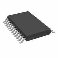
AD8403ARU100-REEL Analog Devices Inc, AD8403ARU100-REEL Datasheet - Page 7

AD8403ARU100-REEL
Manufacturer Part Number
AD8403ARU100-REEL
Description
IC POT DIG QUAD 100K 8B 24TSSOP
Manufacturer
Analog Devices Inc
Datasheet
1.AD8400ARZ1.pdf
(32 pages)
Specifications of AD8403ARU100-REEL
Rohs Status
RoHS non-compliant
Taps
256
Resistance (ohms)
100K
Number Of Circuits
4
Temperature Coefficient
500 ppm/°C Typical
Memory Type
Volatile
Interface
SPI, 3-Wire Serial
Voltage - Supply
2.7 V ~ 5.5 V
Operating Temperature
-40°C ~ 125°C
Mounting Type
Surface Mount
Package / Case
24-TSSOP
Resistance In Ohms
100K
Number Of Elements
4
# Of Taps
256
Resistance (max)
100KOhm
Power Supply Requirement
Single
Interface Type
Serial (3-Wire/SPI)
Single Supply Voltage (typ)
3/5V
Dual Supply Voltage (typ)
Not RequiredV
Single Supply Voltage (min)
2.7V
Single Supply Voltage (max)
5.5V
Dual Supply Voltage (min)
Not RequiredV
Dual Supply Voltage (max)
Not RequiredV
Operating Temp Range
-40C to 125C
Operating Temperature Classification
Automotive
Mounting
Surface Mount
Pin Count
24
Package Type
TSSOP
For Use With
AD8403EVAL - BOARD EVAL FOR AD8403
Lead Free Status / Rohs Status
Not Compliant
Available stocks
Company
Part Number
Manufacturer
Quantity
Price
Company:
Part Number:
AD8403ARU100-REEL
Manufacturer:
A/D
Quantity:
280
Part Number:
AD8403ARU100-REEL
Manufacturer:
ADI/亚德诺
Quantity:
20 000
Parameter
DYNAMIC CHARACTERISTICS
1
2
3
4
5
6
7
8
9
10
11
Typicals represent average readings at 25°C and V
Resistor position nonlinearity error R-INL is the deviation from an ideal value measured between the maximum resistance and the minimum resistance wiper
positions. R-DNL measures the relative step change from ideal between successive tap positions. Parts are guaranteed monotonic. See the test circuit in Figure 38.
I
V
INL and DNL are measured at VW with the RDAC configured as a potentiometer divider similar to a voltage output D/A converter. V
DNL specification limits of ±1 LSB maximum are guaranteed monotonic operating conditions. See the test circuit in Figure 37.
Resistor Terminal A, Resistor Terminal B, and Resistor Terminal W have no limitations on polarity with respect to each other.
Guaranteed by design and not subject to production test. Resistor-terminal capacitance tests are measured with 2.5 V bias on the measured terminal. The remaining
resistor terminals are left open circuit.
Measured at the Ax terminals. All Ax terminals are open-circuited in shutdown mode.
Worst-case supply current consumed when input logic level at 2.4 V, standard characteristic of CMOS logic. See Figure 28 for a plot of I
P
W
All dynamic characteristics use V
Measured at a V
AB
DISS
Bandwidth −3 dB
Total Harmonic Distortion
V
Resistor Noise Voltage
Crosstalk
= V
W
= V
is calculated from (I
Settling Time
DD
DD
/R for V
, wiper (V
11
DD
W
= 3 V or 5 V for the 50 kΩ and 100 kΩ versions.
W
pin where an adjacent V
) = no connect.
DD
× V
DD
). CMOS logic level inputs result in minimum power dissipation.
DD
6, 10
= 5 V.
W
Symbol
BW_50 K
BW_100 K
THD
t
t
e
e
C
S
S
pin is making a full-scale voltage change.
NWB
NWB
T
_50 K
_100 K
_50 K
_100 K
W
DD
= 5 V.
Conditions
R = 50 kΩ
R = 100 kΩ
V
V
V
R
R
V
WB
WB
A
A
A
A
= 1 V rms + 2 V dc, V
= V
= V
= V
= 25 kΩ, f = 1 kHz, RS = 0
= 50 kΩ, f = 1 kHz, RS = 0
DD
DD
DD
, V
, V
, V
Rev. E | Page 7 of 32
B
B
B
= 0 V, ±1% error band
= 0 V, ±1% error band
= 0 V
B
= 2 V dc, f = 1 kHz
Min
AD8400/AD8402/AD8403
A
= V
Typ
125
71
0.003
9
18
20
29
−65
DD
DD
vs. logic voltage.
and V
1
B
= 0 V.
Max
Unit
kHz
kHz
%
μs
μs
nV/√Hz
nV/√Hz
dB


