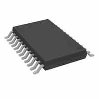
AD8403ARU1 Analog Devices Inc, AD8403ARU1 Datasheet - Page 11

AD8403ARU1
Manufacturer Part Number
AD8403ARU1
Description
IC POT DIG QUAD 1K 8BIT 24TSSOP
Manufacturer
Analog Devices Inc
Datasheet
1.AD8400ARZ1.pdf
(32 pages)
Specifications of AD8403ARU1
Rohs Status
RoHS non-compliant
Taps
256
Resistance (ohms)
1K
Number Of Circuits
4
Temperature Coefficient
500 ppm/°C Typical
Memory Type
Volatile
Interface
SPI, 3-Wire Serial
Voltage - Supply
2.7 V ~ 5.5 V
Operating Temperature
-40°C ~ 125°C
Mounting Type
Surface Mount
Package / Case
24-TSSOP
Resistance In Ohms
1.00K
For Use With
AD8403EVAL - BOARD EVAL FOR AD8403
Available stocks
Company
Part Number
Manufacturer
Quantity
Price
Part Number:
AD8403ARU1
Manufacturer:
ADI/亚德诺
Quantity:
20 000
Company:
Part Number:
AD8403ARU1-REEL
Manufacturer:
POWER-ONE
Quantity:
18
Part Number:
AD8403ARU1-REEL
Manufacturer:
ADI/亚德诺
Quantity:
20 000
Company:
Part Number:
AD8403ARU10
Manufacturer:
FUJ
Quantity:
1 000
Part Number:
AD8403ARU10
Manufacturer:
ADI/亚德诺
Quantity:
20 000
Company:
Part Number:
AD8403ARU100
Manufacturer:
STANLEY
Quantity:
6 661
Part Number:
AD8403ARU100
Manufacturer:
ADI/亚德诺
Quantity:
20 000
Company:
Part Number:
AD8403ARU100-REEL
Manufacturer:
A/D
Quantity:
280
Part Number:
AD8403ARU100-REEL
Manufacturer:
ADI/亚德诺
Quantity:
20 000
ABSOLUTE MAXIMUM RATINGS
T
Table 5.
Parameter
V
V
Maximum Current
Digital Input and Output Voltage
Operating Temperature Range
Maximum Junction Temperature
Storage Temperature
Lead Temperature (Soldering, 10 sec)
Package Power Dissipation
Thermal Resistance (θ
1
ESD CAUTION
ESD (electrostatic discharge) sensitive device. Electrostatic charges as high as 4000 V readily accumulate on the
human body and test equipment and can discharge without detection. Although this product features
proprietary ESD protection circuitry, permanent damage may occur on devices subjected to high energy
electrostatic discharges. Therefore, proper ESD precautions are recommended to avoid performance
degradation or loss of functionality.
Maximum terminal current is bounded by the maximum applied voltage
across any two of the A, B, and W terminals at a given resistance, the maximum
current handling of the switches, and the maximum power dissipation of the
package; VDD = 5 V.
DD
A
A
, V
I
I
I
SOIC (R-8)
PDIP (N-14)
PDIP (N-24)
SOIC (R-14)
SOIC (R-24)
TSSOP-14 (RU-14)
TSSOP-24 (RU-24)
I
to GND
(T
WB
WB
WA
AB
= 25°C, unless otherwise noted.
to GND
B
J
, I
50 kΩ/100 kΩ)
, V
Continuous (R
Continuous (R
Continuous (R
Maximum)
WA
W
Pulsed
to GND
WB
WA
AB
1
≤ 1 kΩ, A Open)
≤ 1 kΩ, B Open)
= 1 kΩ/10 kΩ/
JA
)
1
1
Rating
−0.3 V, +8 V
0 V, V
±20 mA
±5 mA
±5 mA
±2.1 mA/±2.1 mA/
0 V, 7 V
−40°C to +125°C
150°C
−65°C to +150°C
300°C
(T
158°C/W
83°C/W
63°C/W
120°C/W
70°C/W
180°C/W
143°C/W
J
±540 μA/±540 μA
max − T
DD
A
)/θ
JA
Rev. E | Page 11 of 32
Stresses above those listed under Absolute Maximum Ratings
may cause permanent damage to the device. This is a stress
rating only; functional operation of the device at these or any
other conditions above those indicated in the operational
section of this specification is not implied. Exposure to absolute
maximum rating conditions for extended periods may affect
device reliability.
SERIAL DATA-WORD FORMAT
Table 6.
B9
A1
MSB
2
9
ADDR
B8
A0
LSB
2
8
B7
D7
MSB
2
7
B6
D6
AD8400/AD8402/AD8403
B5
D5
D4
B4
DATA
B3
D3
B2
D2
B1
D1
B0
D0
LSB
2
0


