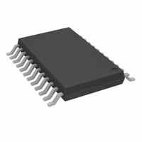
AD8403ARU1 Analog Devices Inc, AD8403ARU1 Datasheet - Page 7

AD8403ARU1
Manufacturer Part Number
AD8403ARU1
Description
IC POT DIG QUAD 1K 8BIT 24TSSOP
Manufacturer
Analog Devices Inc
Datasheet
1.AD8400ARZ1.pdf
(32 pages)
Specifications of AD8403ARU1
Rohs Status
RoHS non-compliant
Taps
256
Resistance (ohms)
1K
Number Of Circuits
4
Temperature Coefficient
500 ppm/°C Typical
Memory Type
Volatile
Interface
SPI, 3-Wire Serial
Voltage - Supply
2.7 V ~ 5.5 V
Operating Temperature
-40°C ~ 125°C
Mounting Type
Surface Mount
Package / Case
24-TSSOP
Resistance In Ohms
1.00K
For Use With
AD8403EVAL - BOARD EVAL FOR AD8403
Available stocks
Company
Part Number
Manufacturer
Quantity
Price
Part Number:
AD8403ARU1
Manufacturer:
ADI/亚德诺
Quantity:
20 000
Company:
Part Number:
AD8403ARU1-REEL
Manufacturer:
POWER-ONE
Quantity:
18
Part Number:
AD8403ARU1-REEL
Manufacturer:
ADI/亚德诺
Quantity:
20 000
Company:
Part Number:
AD8403ARU10
Manufacturer:
FUJ
Quantity:
1 000
Part Number:
AD8403ARU10
Manufacturer:
ADI/亚德诺
Quantity:
20 000
Company:
Part Number:
AD8403ARU100
Manufacturer:
STANLEY
Quantity:
6 661
Part Number:
AD8403ARU100
Manufacturer:
ADI/亚德诺
Quantity:
20 000
Company:
Part Number:
AD8403ARU100-REEL
Manufacturer:
A/D
Quantity:
280
Part Number:
AD8403ARU100-REEL
Manufacturer:
ADI/亚德诺
Quantity:
20 000
Parameter
DYNAMIC CHARACTERISTICS
1
2
3
4
5
6
7
8
9
10
11
Typicals represent average readings at 25°C and V
Resistor position nonlinearity error R-INL is the deviation from an ideal value measured between the maximum resistance and the minimum resistance wiper
positions. R-DNL measures the relative step change from ideal between successive tap positions. Parts are guaranteed monotonic. See the test circuit in Figure 38.
I
V
INL and DNL are measured at VW with the RDAC configured as a potentiometer divider similar to a voltage output D/A converter. V
DNL specification limits of ±1 LSB maximum are guaranteed monotonic operating conditions. See the test circuit in Figure 37.
Resistor Terminal A, Resistor Terminal B, and Resistor Terminal W have no limitations on polarity with respect to each other.
Guaranteed by design and not subject to production test. Resistor-terminal capacitance tests are measured with 2.5 V bias on the measured terminal. The remaining
resistor terminals are left open circuit.
Measured at the Ax terminals. All Ax terminals are open-circuited in shutdown mode.
Worst-case supply current consumed when input logic level at 2.4 V, standard characteristic of CMOS logic. See Figure 28 for a plot of I
P
W
All dynamic characteristics use V
Measured at a V
AB
DISS
Bandwidth −3 dB
Total Harmonic Distortion
V
Resistor Noise Voltage
Crosstalk
= V
W
= V
is calculated from (I
Settling Time
DD
DD
/R for V
, wiper (V
11
DD
W
= 3 V or 5 V for the 50 kΩ and 100 kΩ versions.
W
pin where an adjacent V
) = no connect.
DD
× V
DD
). CMOS logic level inputs result in minimum power dissipation.
DD
6, 10
= 5 V.
W
Symbol
BW_50 K
BW_100 K
THD
t
t
e
e
C
S
S
pin is making a full-scale voltage change.
NWB
NWB
T
_50 K
_100 K
_50 K
_100 K
W
DD
= 5 V.
Conditions
R = 50 kΩ
R = 100 kΩ
V
V
V
R
R
V
WB
WB
A
A
A
A
= 1 V rms + 2 V dc, V
= V
= V
= V
= 25 kΩ, f = 1 kHz, RS = 0
= 50 kΩ, f = 1 kHz, RS = 0
DD
DD
DD
, V
, V
, V
Rev. E | Page 7 of 32
B
B
B
= 0 V, ±1% error band
= 0 V, ±1% error band
= 0 V
B
= 2 V dc, f = 1 kHz
Min
AD8400/AD8402/AD8403
A
= V
Typ
125
71
0.003
9
18
20
29
−65
DD
DD
vs. logic voltage.
and V
1
B
= 0 V.
Max
Unit
kHz
kHz
%
μs
μs
nV/√Hz
nV/√Hz
dB


