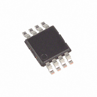
DS3902U-530+T&R Maxim Integrated Products, DS3902U-530+T&R Datasheet

DS3902U-530+T&R
Specifications of DS3902U-530+T&R
Related parts for DS3902U-530+T&R
DS3902U-530+T&R Summary of contents
Page 1
... Wide Operating Voltage (2.4V to 5.5V) ♦ Software Write Protection ♦ User-EEPROM Memory ♦ Programmable Slave Address ♦ Operating Temperature Range: -40°C to +95°C ♦ Small 8-Pin µSOP Package Applications PART DS3902U-530 DS3902U-515 Ordering Information continued at end of data sheet. IN IN- TX_DISABLE TX_FAULT DS3902 ...
Page 2
Dual, NV, Variable Resistors with User EEPROM ABSOLUTE MAXIMUM RATINGS Voltage Range SDA, SCL, H0, CC and H1 Relative to Ground................................-0.5V to +6.0V Voltage Range on ADD_SEL Relative to Ground ...............-0. 0.5V), not to ...
Page 3
AC ELECTRICAL CHARACTERISTICS (Figure +2.4V to +5.5V -40°C to +95°C, unless otherwise noted. Timing referenced PARAMETER SYMBOL SCL Clock Frequency Bus Free Time Between STOP and START Conditions Hold Time (Repeated) ...
Page 4
Dual, NV, Variable Resistors with User EEPROM (V = +3.3V +25°C, unless otherwise noted STANDBY SUPPLY CURRENT vs. TEMPERATURE 180 V = +5V CC 160 140 120 100 ASEL ...
Page 5
T = +25°C, unless otherwise noted ABSOLUTE LINEARITY vs. POSITION 0.1 0.09 0.08 0.07 0.06 0.05 0.04 0.03 0.02 0. 100 POSITION (DEC) H1 ABSOLUTE LINEARITY vs. POSITION 0.1 0.08 0.06 ...
Page 6
Dual, NV, Variable Resistors with User EEPROM Pin Description PIN NAME FUNCTION 1 H0 Resistor 0 High Terminal Serial-Data Open-Drain 2 SDA Input/Output 2 3 SCL I C Serial-Clock Input 4 GND Ground 5 ADD_SEL Address Select ...
Page 7
Table 1. Memory Map DESCRIPTION ADDR MSB Slave Address 00h Configuration 01h X Resistor 0 02h b7 Resistor 1 03h b7 04h Password Entry 05h 06h Password Setting 07h No 08h– Memory 0Fh User 10h– 16 BYTES OF GENERAL PURPOSE ...
Page 8
Dual, NV, Variable Resistors with User EEPROM SDA t BUF t LOW SCL t HD:STA STOP START NOTE: TIMING IS REFERENCED TO V (MAX) AND V (MIN Figure Timing Diagram START Condition: A START ...
Page 9
Slave Address Byte: Each slave on the I responds to a slave addressing byte sent immediately following a START condition. The slave address byte contains the slave address in the most significant 7-bits and the R/W bit in the least ...
Page 10
Dual, NV, Variable Resistors with User EEPROM TYPICAL 2-WIRE WRITE TRANSACTION MSB LSB START R/W READ/ SLAVE WRITE ADDRESS* EXAMPLE 2-WIRE TRANSACTIONS (WHEN ADD_SEL TIED TO GND) A2h A) SINGLE BYTE WRITE START ...
Page 11
... DS3902U-515+T&R 15kΩ, 50kΩ DS3902U-530+ 30kΩ, 50kΩ DS3902U-530+T&R 30kΩ, 50kΩ DS3902U-530/T&R 30kΩ, 50kΩ +Denotes lead-free package. T&R denotes tape-and-reel package. Chip Topology TRANSISTOR COUNT: 11252 SUBSTRATE CONNECTED TO GROUND Maxim cannot assume responsibility for use of any circuitry other than circuitry entirely embodied in a Maxim product. No circuit patent licenses are implied ...


