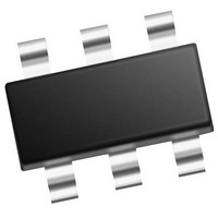
PIC10F220-E/OT Microchip Technology, PIC10F220-E/OT Datasheet - Page 28

PIC10F220-E/OT
Manufacturer Part Number
PIC10F220-E/OT
Description
384B Flash, 16B RAM, 4 I/O, 8bit ADC 6 SOT-23 BAG
Manufacturer
Microchip Technology
Series
PIC® 10Fr
Datasheet
1.PIC10F220-IMC.pdf
(86 pages)
Specifications of PIC10F220-E/OT
Processor Series
PIC10F
Core
RISC
Data Bus Width
8 bit
Program Memory Type
Flash
Program Memory Size
256 B
Data Ram Size
16 B
Interface Type
RS-232, USB
Maximum Clock Frequency
8 MHZ
Number Of Programmable I/os
4
Number Of Timers
1
Maximum Operating Temperature
+ 125 C
Mounting Style
SMD/SMT
Package / Case
SOT-23-6
Operating Temperature Range
- 40 C to + 125 C
Processor To Be Evaluated
PIC10F220
Supply Current (max)
100 nA
Core Processor
PIC
Core Size
8-Bit
Speed
8MHz
Connectivity
-
Peripherals
POR, WDT
Number Of I /o
4
Eeprom Size
-
Ram Size
16 x 8
Voltage - Supply (vcc/vdd)
2 V ~ 5.5 V
Data Converters
A/D 2x8b
Oscillator Type
Internal
Operating Temperature
-40°C ~ 125°C
Lead Free Status / Rohs Status
Details
PIC10F220/222
FIGURE 6-3:
TABLE 6-1:
6.1
When an external clock input is used for Timer0, it must
meet certain requirements. The external clock require-
ment is due to internal phase clock (T
tion. Also, there is a delay in the actual incrementing of
Timer0 after synchronization.
DS41270E-page 26
01h
N/A
N/A
Legend:
Address
PC
(Program
Counter)
Instruction
Timer0
Instruction
Executed
Fetch
Note 1: The TRIS of the T0CKI pin is overridden when T0CS = 1
Using Timer0 With An External
Clock
Shaded cells not used by Timer0, – = unimplemented, x = unknown, u = unchanged.
TMR0
OPTION
TRISGPIO
Q1 Q2 Q3 Q4 Q1 Q2 Q3 Q4 Q1 Q2 Q3 Q4 Q1 Q2 Q3 Q4 Q1 Q2 Q3 Q4 Q1 Q2 Q3 Q4 Q1 Q2 Q3 Q4 Q1 Q2 Q3 Q4
T0
PC-1
Name
REGISTERS ASSOCIATED WITH TIMER0
(1)
TIMER0 TIMING: INTERNAL CLOCK/PRESCALE 1:2
MOVWF TMR0 MOVF TMR0,W MOVF TMR0,W MOVF TMR0,W MOVF TMR0,W MOVF TMR0,W
Timer0 – 8-Bit Real-Time Clock/Counter
T0 + 1
GPWU
PC
Bit 7
—
OSC
GPPU
Bit 6
Write TMR0
executed
—
) synchroniza-
PC + 1
T0CS
Bit 5
—
Read TMR0
reads NT0
PC + 2
T0SE
Bit 4
—
I/O Control Register
Bit 3
PSA
6.1.1
When no prescaler is used, the external clock input is
the same as the prescaler output. The synchronization
of T0CKI with the internal phase clocks is accom-
plished by sampling the prescaler output on the Q2 and
Q4 cycles of the internal phase clocks (Figure 6-4).
Therefore, it is necessary for T0CKI to be high for at
least 2T
for at least 2T
Refer to the electrical specification of the desired
device.
When a prescaler is used, the external clock input is
divided by the asynchronous ripple counter-type
prescaler, so that the prescaler output is symmetrical.
For the external clock to meet the sampling require-
ment, the ripple counter must be taken into account.
Therefore, it is necessary for T0CKI to have a period of
at least 4T
by the prescaler value. The only requirement on T0CKI
high and low time is that they do not violate the
minimum pulse width requirement of Tt0H. Refer to
parameters 40, 41 and 42 in the electrical specification
of the desired device.
Read TMR0
reads NT0
NT0
PC + 3
Bit 2
PS2
OSC
OSC
EXTERNAL CLOCK
SYNCHRONIZATION
(and a small RC delay of 2Tt0H) and low
Bit 1
Read TMR0
reads NT0
PS1
OSC
(and a small RC delay of 4Tt0H) divided
PC + 4
(and a small RC delay of 2Tt0H).
Bit 0
PS0
© 2007 Microchip Technology Inc.
Read TMR0
reads NT0 + 1
xxxx xxxx
1111 1111
---- 1111
Power-On
PC + 5
Value on
Reset
Read TMR0
reads NT0 + 2
NT0 + 1
uuuu uuuu
1111 1111
---- 1111
PC + 6
All Other
Value on
Resets


