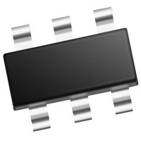
PIC10F220-E/OT Microchip Technology, PIC10F220-E/OT Datasheet - Page 32

PIC10F220-E/OT
Manufacturer Part Number
PIC10F220-E/OT
Description
384B Flash, 16B RAM, 4 I/O, 8bit ADC 6 SOT-23 BAG
Manufacturer
Microchip Technology
Series
PIC® 10Fr
Datasheet
1.PIC10F220-IMC.pdf
(86 pages)
Specifications of PIC10F220-E/OT
Processor Series
PIC10F
Core
RISC
Data Bus Width
8 bit
Program Memory Type
Flash
Program Memory Size
256 B
Data Ram Size
16 B
Interface Type
RS-232, USB
Maximum Clock Frequency
8 MHZ
Number Of Programmable I/os
4
Number Of Timers
1
Maximum Operating Temperature
+ 125 C
Mounting Style
SMD/SMT
Package / Case
SOT-23-6
Operating Temperature Range
- 40 C to + 125 C
Processor To Be Evaluated
PIC10F220
Supply Current (max)
100 nA
Core Processor
PIC
Core Size
8-Bit
Speed
8MHz
Connectivity
-
Peripherals
POR, WDT
Number Of I /o
4
Eeprom Size
-
Ram Size
16 x 8
Voltage - Supply (vcc/vdd)
2 V ~ 5.5 V
Data Converters
A/D 2x8b
Oscillator Type
Internal
Operating Temperature
-40°C ~ 125°C
Lead Free Status / Rohs Status
Details
PIC10F220/222
7.7
The ADRES register contains the results of the last
conversion. These results are present during the sam-
pling period of the next analog conversion process.
After the sampling period is over, ADRES is cleared (=
0). A ‘leading one’ is then right shifted into the ADRES
to serve as an internal conversion complete bit. As
each bit weight, starting with the MSb, is converted, the
leading one is shifted right and the converted bit is
stuffed into ADRES. After a total of 9 right shifts of the
‘leading one’ have taken place, the conversion is com-
plete; the ‘leading one’ has been shifted out and the
GO/DONE bit is cleared.
If the GO/DONE bit is cleared in software during a con-
version, the conversion stops. The data in ADRES is
the partial conversion result. This data is valid for the bit
weights that have been converted. The position of the
‘leading one’ determines the number of bits that have
been converted. The bits that were not converted
before the GO/DONE was cleared are unrecoverable.
REGISTER 7-1:
DS41270E-page 30
bit 7
Legend:
R = Readable bit
-n = Value at POR
bit 7
bit 6
bit 5-4
bit 3-2
bit 1
bit 0
Note 1:
R/W-1
ANS1
2:
3:
4:
Analog Conversion Result
Register
When the ANS bits are set, the channel(s) selected are automatically forced into analog mode regardless of the pin
function previously defined.
CHS<1:0> bits default to 11 after any Reset.
If the ADON bit is clear, the GO/DONE bit cannot be set.
The ANS<1:0> bits are active regardless of the condition of ADON
ANS1: ADC Analog Input Pin Select bit
1 = GP1/AN1 configured for analog input
0 = GP1/AN1 configured as digital I/O
ANS0: ADC Analog Input Pin Select bit
1 = GP0/AN0 configured as an analog input
0 = GP0/AN0 configured as digital I/O
Unimplemented: Read as ‘0’
CHS<1:0>: ADC Channel Select bits
00 = Channel 00 (GP0/AN0)
01 = Channel 01 (GP1/AN1)
1X = 0.6V absolute Voltage reference
GO/DONE: ADC Conversion Status bit
1 = ADC conversion in progress. Setting this bit starts an ADC conversion cycle. This bit is automatically cleared
0 = ADC conversion completed/not in progress. Manually clearing this bit while a conversion is in process
ADON: ADC Enable bit
1 = ADC module is operating
0 = ADC module is shut-off and consumes no power
R/W-1
ANS0
terminates the current conversion.
by hardware when the ADC is done converting.
ADCON0: A/D CONVERTER 0 REGISTER
W = Writable bit
‘1’ = Bit is set
U-0
—
(3)
U-0
—
(4)
(1), (2)
U = Unimplemented bit, read as ‘0’
‘0’ = Bit is cleared
R/W-1
CHS1
7.8
The function of the Internal Absolute Voltage Refer-
ence is to provide a constant voltage for conversion
across the devices V
verter is ratiometric with the conversion reference
voltage being V
0.6V (typical) will result in a result based on the voltage
applied to V
of this reference across the V
approximated by: Conversion Result = 0.6V/(V
Note:
Internal Absolute Voltage
Reference
The actual value of the Absolute Voltage
Reference varies with temperature and
part-to-part variation. The conversion is
also susceptible to analog noise on the
V
ing or sourcing of current on the I/O pins.
DD
DD
R/W-1
CHS0
of the device. The result of conversion
DD
pin and noise generated by the sink-
. Converting a constant voltage of
DD
© 2007 Microchip Technology Inc.
supply range. The A/D Con-
x = Bit is unknown
GO/DONE
R/W-0
DD
range can be
ADON
R/W-0
DD
/256)
bit 0


