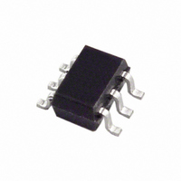
AD5611BKSZ-REEL7 Analog Devices Inc, AD5611BKSZ-REEL7 Datasheet

AD5611BKSZ-REEL7
Specifications of AD5611BKSZ-REEL7
Available stocks
Related parts for AD5611BKSZ-REEL7
AD5611BKSZ-REEL7 Summary of contents
Page 1
FEATURES 6-lead SC70 package Micropower operation: 100 μA maximum Power-down typically to 0.2 μ 2 5.5 V power supply Guaranteed monotonic by design Power-on reset with brownout detection 3 ...
Page 2
AD5601/AD5611/AD5621 TABLE OF CONTENTS Features .............................................................................................. 1 Applications ....................................................................................... 1 General Description ......................................................................... 1 Functional Block Diagram .............................................................. 1 Product Highlights ........................................................................... 1 Revision History ............................................................................... 2 Specifications ..................................................................................... 3 Timing Characteristics ................................................................ 4 Absolute Maximum Ratings ............................................................ 5 ESD ...
Page 3
SPECIFICATIONS kΩ to GND for A/B grades is −40°C to +125°C, typical at 25°C. Table 2. Parameter Min STATIC PERFORMANCE AD5601 Resolution 1 Relative Accuracy (INL) Differential ...
Page 4
AD5601/AD5611/AD5621 Parameter Min POWER REQUIREMENTS V 2 for Normal Mode ±4 ±5 ±2 ±3 for All Power-Down Modes ±4 ...
Page 5
ABSOLUTE MAXIMUM RATINGS T = 25°C, unless otherwise noted. A Table 4. Parameter V to GND DD Digital Input Voltage to GND V to GND OUT Operating Temperature Range Industrial (A/B Grades) Storage Temperature Range Maximum Junction Temperature SC70 Package ...
Page 6
AD5601/AD5611/AD5621 PIN CONFIGURATION AND FUNCTION DESCRIPTIONS Table 5. Pin Function Descriptions Pin No. Mnemonic Description 1 SYNC Level-Triggered Control Input (Active Low). This is the frame synchronization signal for the input data. When SYNC goes low, it enables the input ...
Page 7
TYPICAL PERFORMANCE CHARACTERISTICS 1 REF T = 25°C A 0.5 0 –0.5 –1.0 64 564 1064 1564 2064 2564 DAC CODE Figure 4. Typical AD5621 INL 0 REF ...
Page 8
AD5601/AD5611/AD5621 0. 25°C A 0.15 0.10 0. –0.05 –0.10 –0.15 –0.20 64 564 1064 1564 2064 2564 DAC CODE Figure 10. Typical AD5621 DNL 25°C A ...
Page 9
25°C A CH1 V OUT CH2 CH1 1V, CH2 20mV, TIME BASE = 20µs/DIV Figure 16. Power-On Reset CH1 V DD CH2 V OUT CH1 1V, CH2 5V, TIME ...
Page 10
AD5601/AD5611/AD5621 700 25°C A 600 UNLOADED OUTPUT 500 400 300 MIDSCALE 200 FULL SCALE 100 ZERO SCALE 0 100 1k FREQUENCY (Hz) Figure 22. Noise Spectral Density ...
Page 11
AD5621 MAX TUE 1.1 0.9 0.7 0.5 AD5601 MAX TUE AD5611 MAX TUE 0.3 0.1 –0.1 AD5601 MIN TUE AD5611 MIN TUE –0.3 AD5621 MIN TUE –0.5 –40 – TEMPERATURE (°C) Figure 28. ...
Page 12
AD5601/AD5611/AD5621 1 25°C A 1.3 1.1 0.9 0.7 0.5 AD5611 MAX TUE 0.3 AD5621 MIN TUE 0.1 AD5601 MAX TUE –0.1 AD5611 MIN TUE AD5601 MIN TUE –0.3 2.7 3.2 3.7 4.2 SUPPLY VOLTAGE (V) Figure 34. Total ...
Page 13
TERMINOLOGY Relative Accuracy For the DAC, relative accuracy or integral nonlinearity (INL measure of the maximum deviation, in LSBs, from a straight line passing through the endpoints of the DAC transfer func- tion. See Figure 4 to Figure ...
Page 14
AD5601/AD5611/AD5621 THEORY OF OPERATION DAC SECTION The AD5601/AD5611/AD5621 DACs are fabricated on a CMOS process. The architecture consists of a string DAC followed by an output buffer amplifier. Figure block diagram of the DAC architecture ...
Page 15
DB15 (MSB) PD1 PD0 D11 D10 0 0 NORMAL OPERATION 0 1 1kΩ TO GND 1 0 100kΩ TO GND 1 1 THREE-STATE DB15 (MSB) PD1 PD0 NORMAL OPERATION 0 1 1kΩ TO GND 1 0 ...
Page 16
AD5601/AD5611/AD5621 POWER-ON RESET The AD5601/AD5611/AD5621 contain a power-on reset circuit that controls the output voltage during power-up. The DAC register is filled with 0s and the output voltage remains there until a valid write sequence is ...
Page 17
AD5601/AD5611/AD5621 to Blackfin® ADSP-BF53x Interface Figure 47 shows a serial interface between the AD5601/AD5611/ AD5621 and the Blackfin ADSP-BF53x microprocessor. The ADSP-BF53x processor family incorporates two dual-channel synchronous serial ports, SPORT1 and SPORT0, for serial and multiprocessor communications. Using SPORT0 ...
Page 18
AD5601/AD5611/AD5621 APPLICATIONS CHOOSING A REFERENCE AS POWER SUPPLY FOR THE AD5601/AD5611/AD5621 The AD5601/AD5611/AD5621 come in a tiny SC70 package with less than a 100 μA supply current. Because of this, the choice of reference depends on the application requirements. For ...
Page 19
USING THE AD5601/AD5611/AD5621 WITH A GALVANICALLY ISOLATED INTERFACE In process control applications in industrial environments often necessary to use a galvanically isolated interface to protect and isolate the controlling circuitry from any hazardous common-mode voltages that might occur ...
Page 20
... AD5601BKSZ-REEL7 –40°C to +125°C AD5611AKSZ-500RL7 –40°C to +125°C AD5611AKSZ-REEL7 –40°C to +125°C AD5611BKSZ-500RL7 –40°C to +125°C AD5611BKSZ-REEL7 –40°C to +125°C AD5621AKSZ-500RL7 –40°C to +125°C AD5621AKSZ-REEL7 –40°C to +125°C AD5621BKSZ-500RL7 –40°C to +125°C AD5621BKSZ-REEL7 – ...


