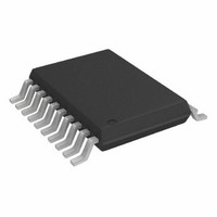
AD5331BRUZ Analog Devices Inc, AD5331BRUZ Datasheet - Page 19

AD5331BRUZ
Manufacturer Part Number
AD5331BRUZ
Description
IC DAC 10BIT SNGL VOUT 20TSSOP
Manufacturer
Analog Devices Inc
Datasheet
1.AD5331BRUZ.pdf
(28 pages)
Specifications of AD5331BRUZ
Data Interface
Parallel
Settling Time
7µs
Number Of Bits
10
Number Of Converters
1
Voltage Supply Source
Single Supply
Power Dissipation (max)
1.25mW
Operating Temperature
-40°C ~ 105°C
Mounting Type
Surface Mount
Package / Case
20-TSSOP
Resolution (bits)
10bit
Sampling Rate
143kSPS
Input Channel Type
Parallel
Supply Voltage Range - Analog
2.5V To 5.5V
Supply Current
140µA
Number Of Channels
1
Resolution
10b
Conversion Rate
143KSPS
Interface Type
Parallel
Single Supply Voltage (typ)
3.3/5V
Dual Supply Voltage (typ)
Not RequiredV
Architecture
Resistor-String
Power Supply Requirement
Single
Output Type
Voltage
Integral Nonlinearity Error
±4LSB
Single Supply Voltage (min)
2.5V
Single Supply Voltage (max)
5.5V
Dual Supply Voltage (min)
Not RequiredV
Dual Supply Voltage (max)
Not RequiredV
Operating Temp Range
-40C to 105C
Operating Temperature Classification
Industrial
Mounting
Surface Mount
Pin Count
20
Package Type
TSSOP
Lead Free Status / RoHS Status
Lead free / RoHS Compliant
Lead Free Status / RoHS Status
Lead free / RoHS Compliant, Lead free / RoHS Compliant
Available stocks
Company
Part Number
Manufacturer
Quantity
Price
Part Number:
AD5331BRUZ
Manufacturer:
ADI/亚德诺
Quantity:
20 000
Part Number:
AD5331BRUZ-REEL7
Manufacturer:
ADI/亚德诺
Quantity:
20 000
POWER-DOWN MODE
The AD5330/AD5331/AD5340/AD5341 have low power
consumption, dissipating only 0.35 mW with a 3 V supply and
0.7 mW with a 5 V supply. Power consumption can be further
reduced when the DAC is not in use by putting it into power-
down mode, which is selected by taking Pin PD low.
When the PD pin is high, the DAC works normally with a
typical power consumption of 140 μA at 5 V (115 μA at 3 V).
In power-down mode, however, the supply current falls to
200 nA at 5 V (80 nA at 3 V) when the DAC is powered down.
Not only does the supply current drop, but the output stage
is also internally switched from the output of the amplifier,
making it open-circuit. This has the advantage that the output
is three-state while the part is in power-down mode and provides
a defined input condition for whatever is connected to the
output of the DAC amplifier. The output stage is illustrated in
Figure 39
Table 9. AD5330/AD5331/AD5340 Truth Table
CLR
1
1
0
1
1
1
1
Table 10. AD5341 Truth Table
CLR
1
1
0
1
1
1
1
1
1
X = don’t care.
X = don’t care.
.
LDAC
1
1
X
1
1
0
0
0
LDAC
1
1
X
1
0
0
CS
1
X
X
0
0
0
0
X
CS
1
X
X
0
0
X
1
WR
X
1
X
0→1
0→1
0→1
0→1
X
WR
X
1
X
0→1
0→1
X
HBEN
X
X
X
0
1
0
1
X
1
Function
No data transfer
No data transfer
Clear all registers
Load input register
Load input register and DAC register
Update DAC register
No data transfer
No data transfer
Clear all registers
Load low byte input register
Load low byte input register and DAC register
Update DAC register
Rev. A | Page 19 of 28
Function
Load high byte input register
Load high byte input register and DAC register
The bias generator, the output amplifier, the resistor string, and
all other associated linear circuitry are shut down when the
power-down mode is activated. However, the contents of the
registers are unaffected when in power-down. The time to exit
power-down is typically 2.5 μs for V
V
when the output voltage deviates from its power-down voltage
(see
DD
= 3 V. This is the time from a rising edge on the PD pin to
Figure 31
STRING DAC
RESISTOR
AD5330/AD5331/AD5340/AD5341
Figure 39. Output Stage During Power-Down
).
AMPLIFIER
DD
POWER-DOWN
= 5 V and 5 μs when
CIRCUITRY
V
OUT


