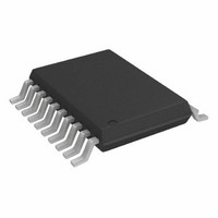
AD5331BRUZ Analog Devices Inc, AD5331BRUZ Datasheet - Page 5

AD5331BRUZ
Manufacturer Part Number
AD5331BRUZ
Description
IC DAC 10BIT SNGL VOUT 20TSSOP
Manufacturer
Analog Devices Inc
Datasheet
1.AD5331BRUZ.pdf
(28 pages)
Specifications of AD5331BRUZ
Data Interface
Parallel
Settling Time
7µs
Number Of Bits
10
Number Of Converters
1
Voltage Supply Source
Single Supply
Power Dissipation (max)
1.25mW
Operating Temperature
-40°C ~ 105°C
Mounting Type
Surface Mount
Package / Case
20-TSSOP
Resolution (bits)
10bit
Sampling Rate
143kSPS
Input Channel Type
Parallel
Supply Voltage Range - Analog
2.5V To 5.5V
Supply Current
140µA
Number Of Channels
1
Resolution
10b
Conversion Rate
143KSPS
Interface Type
Parallel
Single Supply Voltage (typ)
3.3/5V
Dual Supply Voltage (typ)
Not RequiredV
Architecture
Resistor-String
Power Supply Requirement
Single
Output Type
Voltage
Integral Nonlinearity Error
±4LSB
Single Supply Voltage (min)
2.5V
Single Supply Voltage (max)
5.5V
Dual Supply Voltage (min)
Not RequiredV
Dual Supply Voltage (max)
Not RequiredV
Operating Temp Range
-40C to 105C
Operating Temperature Classification
Industrial
Mounting
Surface Mount
Pin Count
20
Package Type
TSSOP
Lead Free Status / RoHS Status
Lead free / RoHS Compliant
Lead Free Status / RoHS Status
Lead free / RoHS Compliant, Lead free / RoHS Compliant
Available stocks
Company
Part Number
Manufacturer
Quantity
Price
Part Number:
AD5331BRUZ
Manufacturer:
ADI/亚德诺
Quantity:
20 000
Part Number:
AD5331BRUZ-REEL7
Manufacturer:
ADI/亚德诺
Quantity:
20 000
TIMING CHARACTERISTICS
V
Table 3.
Parameter
t
t
t
t
t
t
t
t
t
t
t
t
t
1
2
3
1
2
3
4
5
6
7
8
9
10
11
12
13
Guaranteed by design and characterization, not production tested.
All input signals are specified with t
See Figure 2.
DD
= 2.5 V to 5.5 V, all specifications T
Limit at T
0
0
20
5
4.5
5
5
4.5
5
4.5
20
20
50
MIN
R
= t
, T
F
1, 2, 3
= 5 ns (10% to 90% of V
MAX
LDAC
LDAC
DATA,
GAIN,
HBEN
BUF,
CLR
WR
CS
MIN
1
2
NOTES:
1
2
SYNCHRONOUS LDAC UPDATE MODE
ASYNCHRONOUS LDAC UPDATE MODE
to T
MAX
, unless otherwise noted.
t
Figure 2. Parallel Interface Timing Diagram
1
DD
Unit
ns min
ns min
ns min
ns min
ns min
ns min
ns min
ns min
ns min
ns min
ns min
ns min
ns min
) and timed from a voltage level of (V
t
6
t
3
Rev. A | Page 5 of 28
t
t
t
7
9
4
t
2
t
t
Condition/Comments
CS to WR setup time.
CS to WR hold time.
WR pulse width.
Data, GAIN, BUF, HBEN setup time.
Data, GAIN, BUF, HBEN hold time.
Synchronous mode; WR falling to LDAC falling.
Synchronous mode; LDAC falling to WR rising.
Synchronous mode; WR rising to LDAC rising.
Asynchronous mode; LDAC rising to WR rising.
Asynchronous mode; WR rising to LDAC falling.
LDAC pulse width.
CLR pulse width.
Time between WR cycles.
5
8
t
10
t
13
t
11
AD5330/AD5331/AD5340/AD5341
IL
t
12
+ V
IH
)/2.


