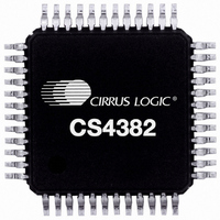
CS4382A-CQZ Cirrus Logic Inc, CS4382A-CQZ Datasheet - Page 28

CS4382A-CQZ
Manufacturer Part Number
CS4382A-CQZ
Description
IC DAC 8CH 114DB 192KHZ 48LQFP
Manufacturer
Cirrus Logic Inc
Specifications of CS4382A-CQZ
Package / Case
48-LQFP
Number Of Bits
24
Data Interface
Serial
Number Of Converters
8
Voltage Supply Source
Analog and Digital
Power Dissipation (max)
680mW
Operating Temperature
-40°C ~ 85°C
Mounting Type
Surface Mount
Conversion Rate
192 KSPS
Resolution
24 bit
Interface Type
Serial
Operating Supply Voltage
5 V
Operating Temperature Range
+ 85 C
Maximum Power Dissipation
390 mW
Mounting Style
SMD/SMT
Number Of Dac Outputs
8
Lead Free Status / RoHS Status
Lead free / RoHS Compliant
For Use With
598-1524 - BOARD EVAL FOR CS4382A DAC
Settling Time
-
Lead Free Status / Rohs Status
Lead free / RoHS Compliant
Other names
598-1061
Available stocks
Company
Part Number
Manufacturer
Quantity
Price
Company:
Part Number:
CS4382A-CQZ
Manufacturer:
Cirrus Logic Inc
Quantity:
10 000
Part Number:
CS4382A-CQZ
Manufacturer:
CRIIUS
Quantity:
20 000
Company:
Part Number:
CS4382A-CQZR
Manufacturer:
Cirrus Logic Inc
Quantity:
10 000
28
4.12
4.12.1 Hardware Mode
4.12.2 Software Mode
Use of the Mute Control function is not mandatory but recommended for designs requiring the absolute min-
imum in extraneous clicks and pops. Also, use of the Mute Control function can enable the system designer
to achieve idle channel noise/signal-to-noise ratios which are only limited by the external mute circuit.
Recommended Power-Up Sequence
1. Hold RST low until the power supplies and configuration pins are stable, and the master and left/right
2. Bring RST high. The device will remain in a low power state with FILT+ low and will initiate the
1. Hold RST low until the power supply is stable, and the master and left/right clocks are locked to the
2. Bring RST high. The device will remain in a low-power state with FILT+ low for 512 LRCK cycles in
3. In order to reduce the chances of clicks and pops, perform a write to the CP_EN bit prior to the
4. Set the PDN bit to 0. This will initiate the power-up sequence, which lasts approximately 50 µs.
clocks are locked to the appropriate frequencies, as discussed in
registers are reset to the default settings, FILT+ will remain low, and VQ will be connected to VA/2.
If RST can not be held low long enough the SDINx pins should remain static low until all other clocks
are stable, and if possible the RST should be toggled low again once the system is stable.
Hardware power-up sequence after approximately 512 LRCK cycles in Single-Speed Mode (1024
LRCK cycles in Double-Speed Mode, and 2048 LRCK cycles in Quad-Speed Mode).
appropriate frequencies, as discussed in
settings; FILT+ will remain low, and VQ will be connected to VA/2.
Single-speed Mode (1024 LRCK cycles in Double-speed Mode, and 2048 LRCK cycles in Quad-
speed Mode).
completion of approximately 512 LRCK cycles in Single-speed Mode (1024 LRCK cycles in Double-
speed Mode, and 2048 LRCK cycles in Quad-speed Mode). The desired register settings can be
loaded while keeping the PDN bit set to 1. Set the RMP_UP and RMP_DN bits to 1; then set the
format and mode control bits to the desired settings.
If more than the stated number of LRCK cycles passes before CPEN bit is written, the chip will enter
Hardware Mode and begin to operate with the M0-M3 as the mode settings. CPEN bit may be written
at anytime, even after the Hardware sequence has begun. It is advised that if the CPEN bit cannot be
set in time, the SDINx pins should remain static low (this way, no audio data can be converted
incorrectly by the Hardware Mode settings).
Figure 17. Recommended Mute Circuitry
Section
4.1. In this state, the registers are reset to the default
Section
4.1. In this state, the
CS4382A
DS618F2


