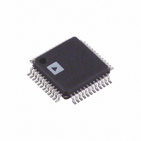
ADV7125KSTZ50 Analog Devices Inc, ADV7125KSTZ50 Datasheet

ADV7125KSTZ50
Specifications of ADV7125KSTZ50
Available stocks
Related parts for ADV7125KSTZ50
ADV7125KSTZ50 Summary of contents
Page 1
FEATURES 330 MSPS throughput rate Triple 8-bit DACs RS-343A-/RS-170-compatible output Complementary outputs DAC output current range: 2 26.5 mA TTL-compatible inputs Internal Reference (1.235 V) Single-supply +5 V/+3.3 V operation 48-lead LQFP and LFCSP packages Low power dissipation ...
Page 2
ADV7125 TABLE OF CONTENTS Features .............................................................................................. 1 Applications....................................................................................... 1 Functional Block Diagram .............................................................. 1 General Description ......................................................................... 1 Product Highlights ........................................................................... 1 Revision History ............................................................................... 2 Specifications..................................................................................... Electrical Characteristics...................................................... 3 3.3 V Electrical Characteristics................................................... ...
Page 3
SPECIFICATIONS 5 V ELECTRICAL CHARACTERISTICS ± 5 1.235 560 Ω REF SET Table 1. Parameter STATIC PERFORMANCE Resolution (Each DAC) Integral Nonlinearity (BSL) Differential Nonlinearity DIGITAL AND CONTROL INPUTS ...
Page 4
ADV7125 3.3 V ELECTRICAL CHARACTERISTICS 1.235 REF SET Table 2. 2 Parameter STATIC PERFORMANCE Resolution (Each DAC) Integral Nonlinearity (BSL) Differential Nonlinearity DIGITAL AND CONTROL INPUTS Input High ...
Page 5
V TIMING SPECIFICATIONS ± 5 1.235 560 Ω REF SET Table 3. 3 Parameter ANALOG OUTPUTS Analog Output Delay 4 Analog Output Rise/Fall Time 5 Analog Output ...
Page 6
ADV7125 3.3 V TIMING SPECIFICATIONS 3 3 1.235 REF SET Table 4. 3 Parameter ANALOG OUTPUTS Analog Output Delay, 4 Analog Output Rise/Fall Time 5 Analog Output Transition Time ...
Page 7
ABSOLUTE MAXIMUM RATINGS Table 5. Parameter V to GND AA Voltage on Any Digital Pin Ambient Operating Temperature ( Storage Temperature ( Junction Temperature ( Lead Temperature (Soldering, 10 sec) Vapor Phase Soldering (1 ...
Page 8
ADV7125 PIN CONFIGURATION AND FUNCTION DESCRIPTIONS Table 6. Pin Function Descriptions Pin Number Mnemonic Description 1, 2, 14, 15, 25, GND Ground. All GND pins must be connected. 26 G7, Red, ...
Page 9
Pin Number Mnemonic Description resistor (R SET signal. Note that the IRE relationships are maintained, regardless of the full-scale output current. The relationship between R is given by: The relationship between R The equation for IOG is ...
Page 10
ADV7125 TERMINOLOGY Blanking Level The level separating the SYNC portion from the video portion of the waveform. Usually referred to as the front porch or back porch IRE units the level that shuts off the picture ...
Page 11
CIRCUIT DESCRIPTION AND OPERATION The ADV7125 contains three 8-bit DACs, with three input channels, each containing an 8-bit register. Also integrated on board the part is a reference amplifier. The CRT control functions, BLANK and SYNC , are integrated on ...
Page 12
ADV7125 Table 7. Typical Video Output Truth Table (R Video Output Level IOG (mA) White Level 26.0 Video Video + 7.2 Video to BLANK Video Black Level 7.2 Black to BLANK 0 BLANK Level 7.2 SYNC Level 0 VIDEO SYNCHRONIZATION ...
Page 13
Figure 5 shows the video waveforms associated with the three RGB outputs driving the doubly terminated 75 Ω load of Figure 6. As well as the gray scale levels (black level to white level), Figure 5 also shows the contributions ...
Page 14
ADV7125 ANALOG SIGNAL INTERCONNECT Place the ADV7125 as close as possible to the output connectors, thus minimizing noise pickup and reflections due to impedance mismatch. The video output signals should overlay the ground plane and not the analog power plane, ...
Page 15
OUTLINE DIMENSIONS 1.45 1.40 1.35 0.15 SEATING 0.05 PLANE VIEW A ROTATED 90° CCW 7.00 BSC SQ PIN 1 INDICATOR VIEW 1.00 12° MAX 0.85 0.80 SEATING PLANE 0.75 1.60 0.60 MAX 0.45 1 0.20 0.09 7° 3.5° 12 0° ...
Page 16
... ADV7125 ORDERING GUIDE Model Temperature Range ADV7125KSTZ50 −40°C to +85°C ADV7125KSTZ50-REEL −40°C to +85°C ADV7125KSTZ140 −40°C to +85°C ADV7125JSTZ240 0°C to +70°C ADV7125JSTZ330 0°C to +70°C ADV7125WBSTZ170 −40°C to +85°C ADV7125WBSTZ170-RL −40°C to +85°C ADV7125BCPZ170 −40°C to +85°C ADV7125BCPZ170-RL − ...


