AD1854JRSZ Analog Devices Inc, AD1854JRSZ Datasheet
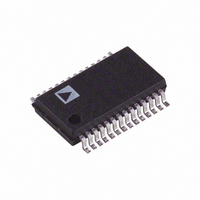
IC DAC STEREO 96KHZ 5V 28SSOP

AD1854JRSZ

Manufacturer Part Number
AD1854JRSZ
Description
IC DAC STEREO 96KHZ 5V 28SSOP
Manufacturer
Analog Devices Inc
Datasheet

Specifications of AD1854JRSZ

Data Interface
DSP, I²S, Serial
Number Of Bits
20
Number Of Converters
2
Voltage Supply Source
Analog and Digital
Power Dissipation (max)
250mW
Operating Temperature
0°C ~ 70°C
Mounting Type
Surface Mount
Package / Case
28-SSOP
Resolution (bits)
20bit
Sampling Rate
96kSPS
Input Channel Type
Serial
Supply Voltage Range - Analog
4.5V To 5.5V
Supply Voltage Range - Digital
4.5V To 5.5V
Lead Free Status / RoHS Status
Lead free / RoHS Compliant
For Use With
EVAL-AD1854EB - BOARD EVAL FOR AD1854
Settling Time
-
Lead Free Status / RoHS Status
Lead free / RoHS Compliant, Lead free / RoHS Compliant

Available stocks

Company
Part Number
Manufacturer
Quantity
Price
Part Number:
AD1854JRSZ
Manufacturer:
ADI
Quantity:
26
Part Number:
AD1854JRSZ
Manufacturer:
ADI/亚德诺
Quantity:
20 000
a
REV. A
Information furnished by Analog Devices is believed to be accurate and
reliable. However, no responsibility is assumed by Analog Devices for its
use, nor for any infringements of patents or other rights of third parties
which may result from its use. No license is granted by implication or
otherwise under any patent or patent rights of Analog Devices.
FEATURES
5 V Stereo Audio DAC System
Accepts 16-/18-/20-/24-Bit Data
Supports 24 Bits and 96 kHz Sample Rate
Multibit Sigma-Delta Modulator with “Perfect Differential
Data Directed Scrambling DAC—Least Sensitive to Jitter
Differential Output for Optimum Performance
113 dB Dynamic Range at 48 kHz Sample Rate
112 dB Signal-to-Noise at 48 kHz Sample Rate
–101 THD+N (AD1854KRS)
On-Chip Volume Control with 1024 Steps
Hardware and Software Controllable Clickless Mute
Zero Input Flag Outputs for Left and Right Channels
Digital De-Emphasis Processing
Supports 256
Switchable Clock Doubler
Power-Down Mode Plus Soft Power-Down Mode
Flexible Serial Data Port with Right-Justified, Left-
28-Lead SSOP Plastic Package
APPLICATIONS
DVD, CD, Set-Top Boxes, Home Theater Systems,
Linearity Restoration” for Reduced Idle Tones and
Noise Floor
(AD1854KRS)
(AD1854KRS)
Justified, and I
Automotive Audio Systems, Sampling Musical
Keyboards, Digital Mixing Consoles, Digital Audio
Effects Processors
16-/18-/20-/24-BIT
DATA INPUT
DIGITAL
SERIAL
MODE
F
2
2
S
S-Compatible
or 384
INTERFACE
SERIAL
DATA
F
S
Master Mode Clock
AD1854
PD/RST
ATTEN/
ATTEN/
MUTE
MUTE
FUNCTIONAL BLOCK DIAGRAM
INTERPOLATOR
INTERPOLATOR
8
8
F
F
MUTE
S
S
VOLUME
MUTE
DELTA MODULATOR
DELTA MODULATOR
SERIAL CONTROL
CONTROL DATA
MULTIBIT SIGMA-
MULTIBIT SIGMA-
DE-EMPHASIS
Stereo, 96 kHz, Multibit
INTERFACE
One Technology Way, P.O. Box 9106, Norwood, MA 02062-9106, U.S.A.
Tel: 781/329-4700
Fax: 781/326-8703
PRODUCT OVERVIEW
The AD1854 is a high performance, single-chip stereo, audio
DAC delivering 113 dB Dynamic Range and 112 dB SNR
(A-weighted—not muted) at 48 kHz sample rate. It is comprised
of a multibit sigma-delta modulator with dither, continuous
time analog filters and analog output drive circuitry. Other features
include an on-chip stereo attenuator and mute, programmed
through an SPI-compatible serial control port. The AD1854
is fully compatible with current DVD formats, including 96 kHz
sample frequency and 24 bits. It is also backwards compatible
by supporting 50 µs/15 µs digital de-emphasis intended for
“redbook” 44.1 kHz sample frequency playback from com-
pact discs.
The AD1854 has a very simple but very flexible serial data input
port that allows for glueless interconnection to a variety of ADCs,
DSP chips, AES/EBU receivers and sample rate converters.
The AD1854 can be configured in left-justified, I
justified. The AD1854 accepts serial audio data in MSB first,
twos-complement format. A power-down mode is offered to mini-
mize power consumption when the device is inactive. The AD1854
operates from a single 5 V power supply. It is fabricated on a single
monolithic integrated circuit and housed in a 28-lead SSOP
package for operation over the temperature range 0°C to 70°C.
INPUT
3
REFERENCE
VOLTAGE
ANALOG
SUPPLY
DAC
DAC
2
World Wide Web Site: http://www.analog.com
DIGITAL
SUPPLY
2
ZERO
FLAG
CLOCK
IN
2
CIRCUIT
CLOCK
OUTPUT
BUFFER
OUTPUT
BUFFER
96/48F
CLOCK
© Analog Devices, Inc., 2000
S
AD1854
ANALOG
OUTPUTS
2
S, and right-
DAC

Related parts for AD1854JRSZ

AD1854JRSZ Summary of contents

Page 1

FEATURES 5 V Stereo Audio DAC System Accepts 16-/18-/20-/24-Bit Data Supports 24 Bits and 96 kHz Sample Rate Multibit Sigma-Delta Modulator with “Perfect Differential Linearity Restoration” for Reduced Idle Tones and Noise Floor Data Directed Scrambling DAC—Least Sensitive to ...

Page 2

AD1854–SPECIFICATIONS TEST CONDITIONS UNLESS OTHERWISE NOTED Supply Voltages ( 5 Ambient Temperature 25°C 12.288 MHz (256 × F Input Clock Input Signal 1.0013 kHz –0.5 dB Full Scale Input Sample Rate 48 kHz Measurement ...

Page 3

POWER Supplies Voltage, Analog and Digital Analog Current Analog Current—Power-Down Digital Current Digital Current—Power-Down Dissipation Operation—Both Supplies Operation—Analog Supply Operation—Digital Supply Power-Down—Both Supplies Power Supply Rejection Ratio 1 kHz 300 mV p-p Signal at Analog Supply Pins 20 kHz 300 ...

Page 4

AD1854 ABSOLUTE MAXIMUM RATINGS* Min DV to DGND –0 AGND –0.3 DD Digital Inputs DGND – 0.3 Analog Outputs AGND – 0.3 AGND to DGND –0.3 Reference Voltage Soldering *Stresses greater than those listed under Absolute Maximum ...

Page 5

Pin Input/Output Pin Name 1 I DGND 2 I MCLK 3 I CLATCH 4 I CCLK 5 I CDATA 6 I 384/256 7 I X2MCLK 8 O ZEROR 9 I DEEMP 10 I 96/48 11 AGND 12 O ...

Page 6

AD1854 OPERATING FEATURES Serial Data Input Port The AD1854’s flexible serial data input port accepts data in twos-complement, MSB-first format. The left channel data field always precedes the right channel data field. The input data consists of either 16, 18, ...

Page 7

L/RCLK LEFT CHANNEL INPUT BCLK INPUT SDATA MSB MSB–1 MSB–2 INPUT L/RCLK LEFT CHANNEL INPUT BCLK INPUT SDATA LSB MSB MSB–1 MSB–2 INPUT t CCP CDATA D15 CCLK t CCH t CCL CLATCH Serial Control Port The AD1854 serial control ...

Page 8

AD1854 CLATCH CCLK CDATA 20 40 CLATCH CCLK CDATA 200 400 Burst Mode To operate with SPI CCLK frequencies up to 12.288 MHz, the SPI port can be operated in Burst Mode. This means that when CLATCH is high, CCLK ...

Page 9

Timing Diagrams The serial data port timing is shown in Figures 9 and 10. The minimum bit clock HI pulsewidth is t DBH clock LO pulsewidth The minimum bit clock period is DBL t . The left/right ...

Page 10

AD1854 SELECT RATE X2MCLK 384/256 96/48 DVDD SPDIF DIRECT DIRECT MCLK/ SEL 10k 10k 10k JP1 SDATA LRCLK AUDIO SCLK DATA MCLK I/F MODE IDPM1 IDPM0 RJ, 16-BIT RJ, 20-BIT ...

Page 11

TYPICAL PERFORMANCE Figures 13 through 20 illustrate the typical analog performance of the AD1854 as measured by an Audio Precision System Two. Signal-to-Noise and THD+N performance are shown under a range of conditions. Figure 14 shows the power supply rejection ...

Page 12

AD1854 0 –10 –20 –30 –40 –50 –60 –70 –80 –90 –100 100 FREQUENCY – kHz Figure 19. Digital Filter Response 0.32 (8.20) 0.29 (7.40) 0.079 (2.0) MAX (0.05) 0 –10 –20 –30 –40 –50 ...

Related keywords