AD7249ANZ Analog Devices Inc, AD7249ANZ Datasheet
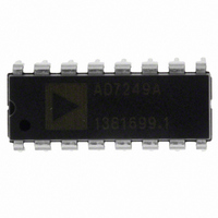
IC DAC 12BIT SRL W/REF 16-DIP

AD7249ANZ

Manufacturer Part Number
AD7249ANZ
Description
IC DAC 12BIT SRL W/REF 16-DIP
Manufacturer
Analog Devices Inc
Series
DACPORT®r
Datasheet

Specifications of AD7249ANZ

Data Interface
Serial
Settling Time
10µs
Number Of Bits
12
Number Of Converters
2
Voltage Supply Source
Dual ±
Power Dissipation (max)
300mW
Operating Temperature
-40°C ~ 85°C
Mounting Type
Through Hole
Package / Case
16-DIP (0.300", 7.62mm)
Resolution (bits)
12bit
Sampling Rate
125kSPS
Input Channel Type
Serial
Supply Current
11mA
Digital Ic Case Style
DIP
No. Of Pins
16
Lead Free Status / RoHS Status
Lead free / RoHS Compliant
a
GENERAL DESCRIPTION
The AD7249 DACPORT contains a pair of 12-bit, voltage-
output, digital-to-analog converters with output amplifiers and
Zener voltage reference on a monolithic CMOS chip. No exter-
nal trims are required to achieve full specified performance.
The output amplifiers are capable of developing +10 V across a
2 kΩ load. The output voltage ranges with single supply opera-
tion are 0 V to +5 V or 0 V to +10 V, while an additional bipolar
± 5 V output range is available with dual supplies. The ranges
are selected using the internal gain resistor.
Interfacing to the AD7249 is serial, minimizing pin count and
allowing a small package size. Standard control signals allow
interfacing to most DSP processors and microcontrollers. The
data stream consists of 16 bits, DB15 to DB13 are don’t care
bits, the 13th bit (DB12) is used as the channel select bit and
the remaining 12 bits (DB11 to DB0) contain the data to update
the DAC. The 16-bit data word is clocked into the input register
on each falling SCLK edge.
The data format is natural binary in both unipolar ranges, while
either offset binary or twos complement format may be selected
in the bipolar range. A CLR function is provided which sets the
output to 0 V in both unipolar ranges and in the twos comple-
ment bipolar range, while with offset binary data format, the
output is set to –REFIN. This function is useful as a power-on
reset as it allows the outputs to be set to a known voltage level.
DACPORT is a registered trademark of Analog Devices, Inc.
The AD7249 features a serial interface which allows easy con-
nection to both microcomputers and 16-bit digital signal proces-
sors with serial ports. The serial data may be applied at rates up
to 2 MHz allowing a DAC update rate of 125 kHz.
The AD7249 is fabricated on linear compatible CMOS
(LC
aged in 16-lead DIP and 16-lead SOIC packages.
PRODUCT HIGHLIGHTS
1. Two complete 12-bit DACPORTs
2. Single or dual supply operation
3. Minimum 3-wire interface to most DSP processors
4. DAC update rate—125 kHz
REFOUT
The AD7249 contains two complete voltage output, 12-bit
DACs in both 16-lead DIP and SOIC packages.
2
REFIN
AGND
DGND
MOS), an advanced, mixed technology process. It is pack-
Dual 12-Bit Serial DACPORT
SCLK
FUNCTIONAL BLOCK DIAGRAM
SDIN
V
DD
INPUT SHIFT REGISTER
SYNC
BIN/COMP CLR
AD7249
12-BIT
DAC A
DAC B
12-BIT
V
SS
AD7249
A1
A2
2R
2R
2R
2R
LDAC
LC
2
MOS
R
V
R
V
OUTA
OUTB
OFSA
OFSB
®

Related parts for AD7249ANZ

AD7249ANZ Summary of contents

Page 1

GENERAL DESCRIPTION The AD7249 DACPORT contains a pair of 12-bit, voltage- output, digital-to-analog converters with output amplifiers and Zener voltage reference on a monolithic CMOS chip. No exter- nal trims are required to achieve full specified performance. The output ...

Page 2

AD7249–SPECIFICATIONS + 100 pF to AGND. All specifications Parameter A Version STATIC PERFORMANCE Resolution 12 ± Relative Accuracy ± 0.9 3 Differential Nonlinearity ± Unipolar ...

Page 3

TIMING CHARACTERISTICS Limit at T MIN Parameter (All Versions 200 150 ...

Page 4

AD7249 PIN FUNCTION DESCRIPTION (DIP & SOIC PIN NUMBERS) Pin Mnemonic Description 11 REFOUT Voltage Reference Output. The internal 5 V analog reference is provided at this pin. To operate the part using its internal reference, REFOUT should be connected ...

Page 5

TERMINOLOGY Bipolar Zero Error Bipolar Zero Error is the voltage measured at V DAC is configured for bipolar output and loaded with all 0s (Twos Complement Coding) or with 1000 0000 0000 (Offset Binary Coding due to a ...

Page 6

AD7249 Internal Reference The AD7249 has an on-chip temperature compensated buried Zener reference which is factory trimmed ± 50 mV. The reference voltage is provided at the REFOUT pin. This refer- ence can be used to provide ...

Page 7

DIGITAL INTERFACE The AD7249 contains an input serial to parallel shift register and a DAC latch for both DAC A and DAC B. A simplified diagram of the input loading circuitry is shown in Figure 7. Serial data on the ...

Page 8

AD7249 t 1 SCLK t 2 SYNC DB15 DB14 DB13 SDIN DON'T DON'T DON'T CARE CARE CARE LDAC CLR TRANSFER FUNCTION The internal scaling resistors provided on the AD7249 allow several output voltage ranges. The part ...

Page 9

Bipolar ( 5 V) Configuration The bipolar configuration for the AD7249, which gives an out- put range of – achieved by connecting The AD7249 must be operated from dual OFSB ...

Page 10

AD7249 MICROPROCESSOR INTERFACING Microprocessor interfacing to the AD7249 is via a serial bus which uses standard protocol compatible with DSP processors and microcontrollers. The communications channel requires a three-wire interface consisting of a clock signal, a data signal and a ...

Page 11

AD7249–68HC11 Interface Figure 14 shows a serial interface between the AD7249 and the 68HC11 microcontroller. SCK of the 68HC11 drives SCLK of the AD7249 while the MOSI output drives the serial data line of the AD7249. The SYNC signal is ...

Page 12

AD7249 DATA OUT CLOCK OUT CONTROLLER SYNC OUT CONTROL OUT 0.200 (5.05) 0.125 (3.18) Wide Body SOIC (R-16) 0.413 (10.50) 0.348 (10.10 0.299 (7.60) 0.291 (7.40) 0.419 (10.65 0.404 (10.26) PIN 1 0.107 (2.72) 0.050 (1.27) ...

Related keywords