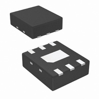
DAC121C081CISD/NOPB National Semiconductor, DAC121C081CISD/NOPB Datasheet - Page 14

DAC121C081CISD/NOPB
Manufacturer Part Number
DAC121C081CISD/NOPB
Description
IC DAC 12BIT MICROPWR I2C 6-LLP
Manufacturer
National Semiconductor
Series
PowerWise®r
Datasheet
1.DAC121C081CISDNOPB.pdf
(24 pages)
Specifications of DAC121C081CISD/NOPB
Settling Time
6µs
Number Of Bits
12
Data Interface
I²C
Number Of Converters
1
Voltage Supply Source
Single Supply
Power Dissipation (max)
730µW
Operating Temperature
-40°C ~ 125°C
Mounting Type
Surface Mount
Package / Case
6-LLP
For Use With
DAC121C08XEB - BOARD EVAL FOR DAC121C081/5
Lead Free Status / RoHS Status
Lead free / RoHS Compliant
Other names
DAC121C081CISD
DAC121C081CISD
DAC121C081CISDTR
DAC121C081CISD
DAC121C081CISDTR
www.national.com
1.0 Functional Description
1.1 DAC SECTION
The DAC121C081 is fabricated on a CMOS process with an
architecture that consists of switches and resistor strings that
are followed by an output buffer.
For simplicity, a single resistor string is shown in Figure 3.
This string consists of 4096 equal valued resistors with a
switch at each junction of two resistors, plus a switch to
ground. The code loaded into the DAC register determines
which switch is closed, connecting the proper node to the
amplifier. The input coding is straight binary with an ideal out-
put voltage of:
where D is the decimal equivalent of the binary code that is
loaded into the DAC register. D can take on any integer value
between 0 and 4095. This configuration guarantees that the
DAC is monotonic.
FIGURE 3. DAC Resistor String
V
OUT
= V
REF
x (D / 4096)
30004907
14
1.2 OUTPUT AMPLIFIER
The output amplifier is rail-to-rail, providing an output voltage
range of 0V to V
even rail-to-rail types, exhibit a loss of linearity as the output
approaches the supply rails (0V and V
reason, linearity is specified over less than the full output
range of the DAC. However, if the reference is less than V
there is only a loss in linearity in the lowest codes. The output
capabilities of the amplifier are described in the Electrical Ta-
bles.
The output amplifiers are capable of driving a load of 2 kΩ in
parallel with 1500 pF to ground or to V
full-scale outputs for given load currents are available in the
Electrical Characteristics Table.
1.3 REFERENCE VOLTAGE
The DAC121C081 uses the supply (V
With that said, V
output will only be as clean as the reference (V
ommended that the reference be driven by a voltage source
with low output impedance.
The DAC121C085 comes with an external reference supply
pin (V
kept as clean as possible.
The Applications section describes a handful of ways to drive
the reference appropriately. Refer to Section 2.1 for details.
REF
). For the DAC121C085, it is important that V
A
A
must be treated as a reference. The Analog
when the reference is V
A
, in this case). For this
A
A
. The zero-code and
) as the reference.
A
. All amplifiers,
A
). It is rec-
REF
be
A
,


