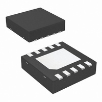
DAC104S085CISD/NOPB National Semiconductor, DAC104S085CISD/NOPB Datasheet - Page 18

DAC104S085CISD/NOPB
Manufacturer Part Number
DAC104S085CISD/NOPB
Description
IC DAC 10BIT QUAD 10-LLP
Manufacturer
National Semiconductor
Series
PowerWise®r
Datasheet
1.DAC104S085CIMMNOPB.pdf
(20 pages)
Specifications of DAC104S085CISD/NOPB
Settling Time
4.5µs
Number Of Bits
10
Data Interface
Serial
Number Of Converters
4
Voltage Supply Source
Single Supply
Power Dissipation (max)
2.5mW
Operating Temperature
-40°C ~ 105°C
Mounting Type
Surface Mount
Package / Case
10-LLP
For Use With
DAC104S085EB - BOARD EVALUATION DAC104S085
Lead Free Status / RoHS Status
Lead free / RoHS Compliant
Other names
DAC104S085CISDTR
Available stocks
Company
Part Number
Manufacturer
Quantity
Price
www.national.com
2.3 DSP/MICROPROCESSOR INTERFACING
Interfacing the DAC104S085 to microprocessors and DSPs
is quite simple. The following guidelines are offered to hasten
the design process.
2.3.1 ADSP-2101/ADSP2103 Interfacing
Figure 10 shows a serial interface between the DAC104S085
and the ADSP-2101/ADSP2103. The DSP should be set to
operate in the SPORT Transmit Alternate Framing Mode. It is
programmed through the SPORT control register and should
be configured for Internal Clock Operation, Active Low Fram-
ing and 16-bit Word Length. Transmission is started by writing
a word to the Tx register after the SPORT mode has been
enabled.
2.3.2 80C51/80L51 Interface
A serial interface between the DAC104S085 and the
80C51/80L51 microcontroller is shown in Figure 11. The
SYNC signal comes from a bit-programmable pin on the mi-
crocontroller. The example shown here uses port line P3.3.
This line is taken low when data is transmitted to the
DAC104S085. Since the 80C51/80L51 transmits 8-bit bytes,
only eight falling clock edges occur in the transmit cycle. To
load data into the DAC, the P3.3 line must be left low after the
first eight bits are transmitted. A second write cycle is initiated
to transmit the second byte of data, after which port line P3.3
is brought high. The 80C51/80L51 transmit routine must rec-
ognize that the 80C51/80L51 transmits data with the LSB first
while the DAC104S085 requires data with the MSB first.
2.3.3 68HC11 Interface
A serial interface between the DAC104S085 and the 68HC11
microcontroller is shown in Figure 12. The SYNC line of the
DAC104S085 is driven from a port line (PC7 in the figure),
similar to the 80C51/80L51.
The 68HC11 should be configured with its CPOL bit as a zero
and its CPHA bit as a one. This configuration causes data on
the MOSI output to be valid on the falling edge of SCLK. PC7
is taken low to transmit data to the DAC. The 68HC11 trans-
FIGURE 10. ADSP-2101/2103 Interface
FIGURE 11. 80C51/80L51 Interface
20195309
20195310
18
mits data in 8-bit bytes with eight falling clock edges. Data is
transmitted with the MSB first. PC7 must remain low after the
first eight bits are transferred. A second write cycle is initiated
to transmit the second byte of data to the DAC, after which
PC7 should be raised to end the write sequence.
2.3.4 Microwire Interface
Figure 13 shows an interface between a Microwire compatible
device and the DAC104S085. Data is clocked out on the rising
edges of the SK signal. As a result, the SK of the Microwire
device needs to be inverted before driving the SCLK of the
DAC104S085.
2.4 LAYOUT, GROUNDING, AND BYPASSING
For best accuracy and minimum noise, the printed circuit
board containing the DAC104S085 should have separate
analog and digital areas. The areas are defined by the loca-
tions of the analog and digital power planes. Both of these
planes should be located in the same board layer. There
should be a single ground plane. A single ground plane is
preferred if digital return current does not flow through the
analog ground area. Frequently a single ground plane design
will utilize a "fencing" technique to prevent the mixing of ana-
log and digital ground current. Separate ground planes should
only be utilized when the fencing technique is inadequate.
The separate ground planes must be connected in one place,
preferably near the DAC104S085. Special care is required to
guarantee that digital signals with fast edge rates do not pass
over split ground planes. They must always have a continu-
ous return path below their traces.
The DAC104S085 power supply should be bypassed with a
10µF and a 0.1µF capacitor as close as possible to the device
with the 0.1µF right at the device supply pin. The 10µF ca-
pacitor should be a tantalum type and the 0.1µF capacitor
should be a low ESL, low ESR type. The power supply for the
DAC104S085 should only be used for analog circuits.
Avoid crossover of analog and digital signals and keep the
clock and data lines on the component side of the board. The
clock and data lines should have controlled impedances.
FIGURE 13. Microwire Interface
FIGURE 12. 68HC11 Interface
20195311
20195312


