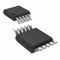
DAC124S085CIMM/NOPB National Semiconductor, DAC124S085CIMM/NOPB Datasheet - Page 14

DAC124S085CIMM/NOPB
Manufacturer Part Number
DAC124S085CIMM/NOPB
Description
IC DAC 12BIT QUAD R-R 10-MSOP
Manufacturer
National Semiconductor
Series
PowerWise®r
Datasheet
1.DAC124S085CIMMNOPB.pdf
(20 pages)
Specifications of DAC124S085CIMM/NOPB
Settling Time
6µs
Number Of Bits
12
Data Interface
DSP, MICROWIRE™, QSPI™, Serial, SPI™
Number Of Converters
4
Voltage Supply Source
Single Supply
Operating Temperature
-40°C ~ 105°C
Mounting Type
Surface Mount
Package / Case
10-MSOP, Micro10™, 10-uMAX, 10-uSOP
Number Of Channels
4
Resolution
12b
Interface Type
Serial (3-Wire, SPI, QSPI, Microwire)
Single Supply Voltage (typ)
3.3/5V
Dual Supply Voltage (typ)
Not RequiredV
Architecture
Resistor-String
Power Supply Requirement
Single
Output Type
Voltage
Integral Nonlinearity Error
±8LSB
Single Supply Voltage (min)
2.7V
Single Supply Voltage (max)
5.5V
Dual Supply Voltage (min)
Not RequiredV
Dual Supply Voltage (max)
Not RequiredV
Operating Temp Range
-40C to 105C
Operating Temperature Classification
Industrial
Mounting
Surface Mount
Pin Count
10
Package Type
MSOP
For Use With
DAC124S085EB - BOARD EVALUATION DAC124S085
Lead Free Status / RoHS Status
Lead free / RoHS Compliant
Power Dissipation (max)
-
Lead Free Status / Rohs Status
Compliant
Other names
DAC124S085CIMM
DAC124S085CIMMTR
DAC124S085CIMMTR
Available stocks
Company
Part Number
Manufacturer
Quantity
Price
Company:
Part Number:
DAC124S085CIMM/NOPB
Manufacturer:
ADI
Quantity:
9 712
www.national.com
1.0 Functional Description
1.1 DAC SECTION
The DAC124S085 is fabricated on a CMOS process with an
architecture that consists of switches and resistor strings that
are followed by an output buffer. The reference voltage is ex-
ternally applied at V
For simplicity, a single resistor string is shown in Figure 3.
This string consists of 4096 equal valued resistors with a
switch at each junction of two resistors, plus a switch to
ground. The code loaded into the DAC register determines
which switch is closed, connecting the proper node to the
amplifier. The input coding is straight binary with an ideal out-
put voltage of:
where D is the decimal equivalent of the binary code that is
loaded into the DAC register. D can take on any value be-
tween 0 and 4095. This configuration guarantees that the
DAC is monotonic.
1.2 OUTPUT AMPLIFIERS
The output amplifiers are rail-to-rail, providing an output volt-
age range of 0V to V
even rail-to-rail types, exhibit a loss of linearity as the output
FIGURE 3. DAC Resistor String
V
OUTA,B,C,D
REFIN
A
when the reference is V
and is shared by all four DACs.
= V
REFIN
x (D / 4096)
A
. All amplifiers,
20173207
14
approaches the supply rails (0V and V
reason, linearity is specified over less than the full output
range of the DAC. However, if the reference is less than V
there is only a loss in linearity in the lowest codes. The output
capabilities of the amplifier are described in the Electrical Ta-
bles.
The output amplifiers are capable of driving a load of 2 kΩ in
parallel with 1500 pF to ground or to V
full-scale outputs for given load currents are available in the
Electrical Characterisics Table.
1.3 RERENCE VOLTAGE
The DAC124S085 uses a single external reference that is
shared by all four channels. The reference pin, V
buffered and has an input impedance of 30 kΩ. It is recom-
mended that V
output impedance. The reference voltage range is 1.0V to
V
1.4 SERIAL INTERFACE
The three-wire interface is compatible with SPI, QSPI and
MICROWIRE, as well as most DSPs and operates at clock
rates up to 40 MHz. See the Timing Diagram for information
on a write sequence.
A write sequence begins by bringing the SYNC line low. Once
SYNC is low, the data on the D
bit serial input register on the falling edges of SCLK. To avoid
misclocking data into the shift register, it is critical that
SYNC not be brought low simultaneously with a falling edge
of SCLK (see Serial Timing Diagram, Figure 2). On the 16th
falling clock edge, the last data bit is clocked in and the pro-
grammed function (a change in the DAC channel address,
mode of operation and/or register contents) is executed. At
this point the SYNC line may be kept low or brought high. Any
data and clock pusles after the 16th falling clock edge will be
ignored. In either case, SYNC must be brought high for the
minimum specified time before the next write sequence is ini-
tiated with a falling edge of SYNC.
Since the SYNC and D
are high, they should be idled low between write sequences
to minimize power consumption.
1.5 INPUT SHIFT REGISTER
The input shift register, Figure 4, has sixteen bits. The first
two bits are address bits. They determine whether the register
data is for DAC A, DAC B, DAC C, or DAC D. The address
bits are followed by two bits that determine the mode of op-
eration (writing to a DAC register without updating the outputs
of all four DACs, writing to a DAC register and updating the
outputs of all four DACs, writing to the register of all four DACs
and updating their outputs, or powering down all four outputs).
The final twelve bits of the shift register are the data bits. The
data format is straight binary (MSB first, LSB last), with all 0's
corresponding to an output of 0V and all 1's corresponding to
a full-scale output of V
input register are transferred to the DAC register on the six-
teenth falling edge of SCLK. See Timing Diagram, Figure 2.
A
, providing the widest possible output dynamic range.
REFIN
be driven by a voltage source with low
REFIN
IN
buffers draw more current when they
- 1 LSB. The contents of the serial
IN
line is clocked into the 16-
A
, in this case). For this
A
. The zero-code and
REFIN
, is not
A
,


