DAC124S085CIMM/NOPB National Semiconductor, DAC124S085CIMM/NOPB Datasheet - Page 3
DAC124S085CIMM/NOPB
Manufacturer Part Number
DAC124S085CIMM/NOPB
Description
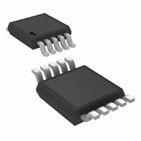
IC DAC 12BIT QUAD R-R 10-MSOP
Manufacturer
National Semiconductor
Series
PowerWise®r
Datasheet
1.DAC124S085CIMMNOPB.pdf
(20 pages)
Specifications of DAC124S085CIMM/NOPB
Settling Time
6µs
Number Of Bits
12
Data Interface
DSP, MICROWIRE™, QSPI™, Serial, SPI™
Number Of Converters
4
Voltage Supply Source
Single Supply
Operating Temperature
-40°C ~ 105°C
Mounting Type
Surface Mount
Package / Case
10-MSOP, Micro10™, 10-uMAX, 10-uSOP
Number Of Channels
4
Resolution
12b
Interface Type
Serial (3-Wire, SPI, QSPI, Microwire)
Single Supply Voltage (typ)
3.3/5V
Dual Supply Voltage (typ)
Not RequiredV
Architecture
Resistor-String
Power Supply Requirement
Single
Output Type
Voltage
Integral Nonlinearity Error
±8LSB
Single Supply Voltage (min)
2.7V
Single Supply Voltage (max)
5.5V
Dual Supply Voltage (min)
Not RequiredV
Dual Supply Voltage (max)
Not RequiredV
Operating Temp Range
-40C to 105C
Operating Temperature Classification
Industrial
Mounting
Surface Mount
Pin Count
10
Package Type
MSOP
For Use With
DAC124S085EB - BOARD EVALUATION DAC124S085
Lead Free Status / RoHS Status
Lead free / RoHS Compliant
Power Dissipation (max)
-
Lead Free Status / Rohs Status
Compliant
Other names
DAC124S085CIMM
DAC124S085CIMMTR
DAC124S085CIMMTR
Available stocks
Company
Part Number
Manufacturer
Quantity
Price
Company:

Part Number:
DAC124S085CIMM/NOPB
Manufacturer:
ADI
Quantity:
9 712


Pin Descriptions
Pin No.
MSOP
LLP
10
11
1
2
3
4
5
6
7
8
9
(LLP only)
Symbol
V
SYNC
V
V
V
V
SCLK
GND
PAD
OUTC
OUTD
REFIN
D
OUTA
OUTB
V
IN
A
Analog Output
Analog Output
Analog Output
Analog Output
Analog Input
Digital Input
Digital Input
Digital Input
Ground
Ground
Supply
Type
Power supply input. Must be decoupled to GND.
Channel A Analog Output Voltage.
Channel B Analog Output Voltage.
Channel C Analog Output Voltage.
Channel D Analog Output Voltage.
Ground reference for all on-chip circuitry.
Unbuffered reference voltage shared by all channels. Must be decoupled
to GND.
Serial Data Input. Data is clocked into the 16-bit shift register on the falling
edges of SCLK after the fall of SYNC.
Frame synchronization input for the data input. When this pin goes low,
it enables the input shift register and data is transferred on the falling
edges of SCLK. The DAC is updated on the 16th clock cycle unless
SYNC is brought high before the 16th clock, in which case the rising edge
of SYNC acts as an interrupt and the write sequence is ignored by the
DAC.
Serial Clock Input. Data is clocked into the input shift register on the
falling edges of this pin.
Exposed die attach pad can be connected to ground or left floating.
Soldering the pad to the PCB offers optimal thermal performance and
enhances package self-alignment during reflow.
3
Description
www.national.com
Related parts for DAC124S085CIMM/NOPB
Image
Part Number
Description
Manufacturer
Datasheet
Request
R

Part Number:
Description:
National Semiconductor [8-Bit D/A Converter]
Manufacturer:
National Semiconductor
Datasheet:
Part Number:
Description:
National Semiconductor [Media Coprocessor]
Manufacturer:
National Semiconductor
Datasheet:
Part Number:
Description:
Digitally Controlled Tone and Volume Circuit with Stereo Audio Power Amplifier, Microphone Preamp Stage and National 3D Sound
Manufacturer:
National Semiconductor
Datasheet:
Part Number:
Description:
Digitally Controlled Tone and Volume Circuit with Stereo Audio Power Amplifier, Microphone Preamp Stage and National 3D Sound
Manufacturer:
National Semiconductor
Datasheet:
Part Number:
Description:
AC97 Rev 2 Codec with Sample Rate Conversion and National 3D Sound
Manufacturer:
National Semiconductor
Part Number:
Description:
Manufacturer:
National Semiconductor
Datasheet:
Part Number:
Description:
Manufacturer:
National Semiconductor
Datasheet:
Part Number:
Description:
General Purpose, Low Voltage, Low Power, Rail-to-Rail Output Operational Amplifiers
Manufacturer:
National Semiconductor
Datasheet:
Part Number:
Description:
8-bit 20 MSPS flash A/D converter.
Manufacturer:
National Semiconductor
Datasheet:
Part Number:
Description:
Low Noise Quad Operational Amplifier
Manufacturer:
National Semiconductor
Datasheet:
Part Number:
Description:
Quad Differential Line Receivers
Manufacturer:
National Semiconductor
Datasheet:
Part Number:
Description:
Quad High Speed Trapezoidal? Bus Transceiver
Manufacturer:
National Semiconductor
Datasheet:
Part Number:
Description:
Dual Line Receiver
Manufacturer:
National Semiconductor
Datasheet:
Part Number:
Description:
TTL to 10k ECL Level Translator with Latch
Manufacturer:
National Semiconductor
Datasheet: