DAC124S085CISD/NOPB National Semiconductor, DAC124S085CISD/NOPB Datasheet - Page 6
DAC124S085CISD/NOPB
Manufacturer Part Number
DAC124S085CISD/NOPB
Description
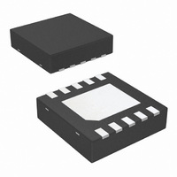
IC DAC 12BIT QUAD R-R 10-LLP
Manufacturer
National Semiconductor
Series
PowerWise®r
Datasheet
1.DAC124S085CIMMNOPB.pdf
(20 pages)
Specifications of DAC124S085CISD/NOPB
Settling Time
6µs
Number Of Bits
12
Data Interface
DSP, MICROWIRE™, QSPI™, Serial, SPI™
Number Of Converters
4
Voltage Supply Source
Single Supply
Operating Temperature
-40°C ~ 105°C
Mounting Type
Surface Mount
Package / Case
10-LLP
Number Of Channels
4
Resolution
12b
Interface Type
Serial (3-Wire, SPI, QSPI, Microwire)
Single Supply Voltage (typ)
3.3/5V
Dual Supply Voltage (typ)
Not RequiredV
Architecture
Resistor-String
Power Supply Requirement
Single
Output Type
Voltage
Integral Nonlinearity Error
±8LSB
Single Supply Voltage (min)
2.7V
Single Supply Voltage (max)
5.5V
Dual Supply Voltage (min)
Not RequiredV
Dual Supply Voltage (max)
Not RequiredV
Operating Temp Range
-40C to 105C
Operating Temperature Classification
Industrial
Mounting
Surface Mount
Pin Count
10
Package Type
LLP EP
For Use With
DAC124S085EB - BOARD EVALUATION DAC124S085
Lead Free Status / RoHS Status
Lead free / RoHS Compliant
Power Dissipation (max)
-
Lead Free Status / Rohs Status
Compliant
Other names
DAC124S085CISDTR
DAC124S085CISDTR
DAC124S085CISDTR
Available stocks
Company
Part Number
Manufacturer
Quantity
Price
Company:

Part Number:
DAC124S085CISD/NOPB
Manufacturer:
NSC
Quantity:
5 128


www.national.com
f
t
SR
t
1/f
t
t
t
t
t
t
t
SCLK
s
WU
CH
CL
SS
DS
DH
CFSR
SYNC
Symbol
A.C. and Timing Characteristics
Values shown in this table are design targets and are subject to change before product release.
The following specifications apply for V
48 to 4047. Boldface limits apply for T
Note 1: Absolute Maximum Ratings indicate limits beyond which damage to the device may occur. Operating Ratings indicate conditions for which the device is
functional, but do not guarantee specific performance limits. For guaranteed specifications and test conditions, see the Electrical Characteristics. The guaranteed
specifications apply only for the test conditions listed. Some performance characteristics may degrade when the device is not operated under the listed test
conditions. Operation of the device beyond the maximum Operating Ratings is not recommended.
Note 2: All voltages are measured with respect to GND = 0V, unless otherwise specified.
Note 3: When the input voltage at any pin exceeds 5.5V or is less than GND, the current at that pin should be limited to 10 mA. The 20 mA maximum package
input current rating limits the number of pins that can safely exceed the power supplies with an input current of 10 mA to two.
Note 4: The absolute maximum junction temperature (T
junction-to-ambient thermal resistance (θ
for maximum power dissipation will be reached only when the device is operated in a severe fault condition (e.g., when input or output pins are driven beyond
the operating ratings, or the power supply polarity is reversed).
Note 5: Human body model is 100 pF capacitor discharged through a 1.5 kΩ resistor. Machine model is 220 pF discharged through ZERO Ohms.
Note 6: Reflow temperature profiles are different for lead-free packages.
Note 7: The inputs are protected as shown below. Input voltage magnitudes up to 5.5V, regardless of V
example, if V
SCLK
SCLK Frequency
Output Voltage Settling Time
(Note 10)
Output Slew Rate
Glitch Impulse
Digital Feedthrough
Digital Crosstalk
DAC-to-DAC Crosstalk
Multiplying Bandwidth
Total Harmonic Distortion
Wake-Up Time
SCLK Cycle Time
SCLK High time
SCLK Low Time
SYNC Set-up Time prior to SCLK
Falling Edge
Data Set-Up Time prior to SCLK
Falling Edge
Data Hold Time after SCLK Falling
Edge
SCLK fall prior to rise of SYNC
SYNC High Time
A
is 3V, the digital input pins can be driven with a 5V logic device.
Parameter
JA
), and the ambient temperature (T
A
MIN
= +2.7V to +5.5V, V
≤
J
max) for this device is 150°C. The maximum allowable power dissipation is dictated by T
T
A
400h to C00h code change
R
Code change from 800h to 7FFh
V
V
input frequency = 10kHz
V
V
≤
REFIN
REFIN
A
A
L
= 2kΩ, C
= V
= V
T
MAX
REF
REF
= 2.5V ± 0.1Vpp
= 2.5V ± 0.1Vpp
and all other limits are at T
= 3V
= 5V
L
REFIN
Conductions
A
= 200 pF
), and can be calculated using the formula P
6
= V
A
, C
L
= 200 pF to GND, f
20173204
A
A
, will not cause errors in the conversion result. For
= 25°C, unless otherwise specified.
(Note 9)
Typical
160
0.5
1.5
1.5
40
12
70
39
25
SCLK
6
1
1
3
6
7
7
4
0
6
D
MAX = (T
= 30 MHz, input code range
(Note 9)
Limits
J
max − T
8.5
3.5
3.5
30
33
10
10
10
10
3
A
) / θ
JA
J
MHz (max)
max, the
µs (max)
. The values
(Limits)
ns (min)
ns (min)
ns (min)
ns (min)
ns (min)
ns (min)
ns (min)
ns (min)
nV-sec
nV-sec
nV-sec
nV-sec
Units
µsec
µsec
V/µs
kHz
dB
Related parts for DAC124S085CISD/NOPB
Image
Part Number
Description
Manufacturer
Datasheet
Request
R

Part Number:
Description:
National Semiconductor [8-Bit D/A Converter]
Manufacturer:
National Semiconductor
Datasheet:
Part Number:
Description:
National Semiconductor [Media Coprocessor]
Manufacturer:
National Semiconductor
Datasheet:
Part Number:
Description:
Digitally Controlled Tone and Volume Circuit with Stereo Audio Power Amplifier, Microphone Preamp Stage and National 3D Sound
Manufacturer:
National Semiconductor
Datasheet:
Part Number:
Description:
Digitally Controlled Tone and Volume Circuit with Stereo Audio Power Amplifier, Microphone Preamp Stage and National 3D Sound
Manufacturer:
National Semiconductor
Datasheet:
Part Number:
Description:
AC97 Rev 2 Codec with Sample Rate Conversion and National 3D Sound
Manufacturer:
National Semiconductor
Part Number:
Description:
Manufacturer:
National Semiconductor
Datasheet:
Part Number:
Description:
Manufacturer:
National Semiconductor
Datasheet:
Part Number:
Description:
General Purpose, Low Voltage, Low Power, Rail-to-Rail Output Operational Amplifiers
Manufacturer:
National Semiconductor
Datasheet:
Part Number:
Description:
8-bit 20 MSPS flash A/D converter.
Manufacturer:
National Semiconductor
Datasheet:
Part Number:
Description:
Low Noise Quad Operational Amplifier
Manufacturer:
National Semiconductor
Datasheet:
Part Number:
Description:
Quad Differential Line Receivers
Manufacturer:
National Semiconductor
Datasheet:
Part Number:
Description:
Quad High Speed Trapezoidal? Bus Transceiver
Manufacturer:
National Semiconductor
Datasheet:
Part Number:
Description:
Dual Line Receiver
Manufacturer:
National Semiconductor
Datasheet:
Part Number:
Description:
TTL to 10k ECL Level Translator with Latch
Manufacturer:
National Semiconductor
Datasheet: