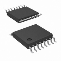
DAC108S085CIMT/NOPB National Semiconductor, DAC108S085CIMT/NOPB Datasheet

DAC108S085CIMT/NOPB
Specifications of DAC108S085CIMT/NOPB
Available stocks
Related parts for DAC108S085CIMT/NOPB
DAC108S085CIMT/NOPB Summary of contents
Page 1
... Ordering Information Order Numbers DAC108S085CISQ DAC108S085CISQX DAC108S085CIMT DAC108S085CIMTX DAC108S085EB SPI ™ trademark of Motorola, Inc. © 2007 National Semiconductor Corporation Features ■ Guaranteed Monotonicity ■ Low Power Operation ■ Rail-to-Rail Voltage Output ■ Daisy Chain Capability ■ ...
Page 2
Block Diagram www.national.com 2 30031203 ...
Page 3
Pin Configuration Pin Descriptions LLP TSSOP Symbol Pin No. Pin No OUTA OUTB OUTC OUTD REF1 REF2 8 ...
Page 4
... Absolute Maximum Ratings If Military/Aerospace specified devices are required, please contact the National Semiconductor Sales Office/ Distributors for availability and specifications. Supply Voltage Voltage on any Input Pin Input Current at Any Pin (Note 3) Package Input Current (Note 3) Power Consumption 25°C A ESD Susceptibility (Note 5) ...
Page 5
Symbol Parameter Output Short Circuit Current (sink (Note 10) Continuous Output Current per I O channel (Note 9) C Maximum Load Capacitance Output Impedance OUT REFERENCE INPUT CHARACTERISTICS Input Range Minimum Input Range Maximum VREF1,2 ...
Page 6
Symbol Parameter Total Power Consumption (output P N unloaded) Total Power Consumption in all PD P Modes, PD (Note 9) A.C. and Timing Characteristics The following specifications apply for 1011. Boldface limits apply for T Symbol Parameter ...
Page 7
Note 1: Absolute Maximum Ratings indicate limits beyond which damage to the device may occur. Operating Ratings indicate conditions for which the device is functional, but do not guarantee specific performance limits. For guaranteed specifications and test conditions, see the ...
Page 8
Specification Definitions DIFFERENTIAL NON-LINEARITY (DNL) is the measure of the maximum deviation from the ideal step size of 1 LSB, which 1024 = V / 1024. REF A DAC-to-DAC CROSSTALK is the glitch impulse transferred to a ...
Page 9
Typical Performance Characteristics unless otherwise stated INL vs Code INL/DNL vs V REF INL/DNL +2.7V to +5.5V REF1,2 30031252 INL/DNL vs f 30031257 INL/DNL vs Temperature 30031222 ...
Page 10
Zero Code Error vs. V Zero Code Error vs. f Full-Scale Error vs. V www.national.com A 30031230 Zero Code Error vs. Temperature SCLK 30031234 A 30031237 10 Zero Code Error vs. V REF 30031231 30031236 Full-Scale Error vs. V REF ...
Page 11
Full-Scale Error vs. f SCLK 30031233 I vs 30031244 I vs. V VREF REF 30031225 Full-Scale Error vs. Temperature I vs. Temperature VA I vs. Temperature VREF 11 30031239 30031245 30031235 www.national.com ...
Page 12
Settling Time Wake-Up Time Power-On Reset www.national.com Glitch Response 30031228 DAC-to-DAC Crosstalk 30031251 Multiplying Bandwidth 30031247 12 30031246 30031238 30031250 ...
Page 13
Functional Description 1.1 DAC ARCHITECTURE The DAC108S085 is fabricated on a CMOS process with an architecture that consists of switches and resistor strings that are followed by an output buffer. The reference voltages are externally applied at V for ...
Page 14
D is active. OUT 1.5 DAISY CHAIN OPERATION Daisy chain operation allows communication with any number of DAC108S085s using a single serial interface. As long as the correct number ...
Page 15
When the DAC108S085 first powers up, the DAC is in WRM. In WRM, the registers of each individual DAC channel can be written to without causing the DAC outputs to be updated. This is accomplished by setting DB15 to "0", ...
Page 16
POWER-ON RESET The power-on reset circuit controls the output voltages of the eight DACs during power-up. Upon application of power, the DAC registers are filled with zeros and the output voltages are set to 0V. The outputs remain at ...
Page 17
LM4132 The LM4132, with its ±0.05% accuracy over temperature good choice as a reference source for the DAC108S085. The 4.096V version is useful 4.095V output range is desirable. Bypassing the LM4132 voltage input ...
Page 18
ESR. Ceramic capacitors are attractive due to their small size but generally have ESR val- ues that are too low for use with the LP2980. Aluminum electrolytic capacitors are typically not a good choice ...
Page 19
ADC Reference shows Channel A of the DAC108S085 providing the drive or supply voltage for a bridge sensor. By having the sensor sup- ply voltage adjustable, the output of the sensor can be opti- mized to the input level ...
Page 20
Programmable Attenuator shows one of the channels of the DAC108S085 being used as a single-quadrant multiplier. In this configuration signal can be driven into one of the reference pins. The SPI interface of the DAC ...
Page 21
LAYOUT, GROUNDING, AND BYPASSING For best accuracy and minimum noise, the printed circuit board containing the DAC108S085 should have separate analog and digital areas. The areas are defined by the loca- tions of the analog and digital power planes. ...
Page 22
Physical Dimensions www.national.com inches (millimeters) unless otherwise noted 16-Lead LLP Order Numbers DAC108S085CISQ NS Package Number SQA16A 16-Lead TSSOP Order Numbers DAC108S085CIMT NS Package Number MTC16 22 ...
Page 23
Notes 23 www.national.com ...
Page 24
... National Semiconductor and the National Semiconductor logo are registered trademarks of National Semiconductor Corporation. All other brand or product names may be trademarks or registered trademarks of their respective holders. ...


