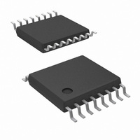
DAC108S085CIMT/NOPB National Semiconductor, DAC108S085CIMT/NOPB Datasheet - Page 3

DAC108S085CIMT/NOPB
Manufacturer Part Number
DAC108S085CIMT/NOPB
Description
IC DAC 10BIT OCTAL R-R 16-TSSOP
Manufacturer
National Semiconductor
Series
PowerWise®r
Datasheet
1.DAC108S085CISQNOPB.pdf
(24 pages)
Specifications of DAC108S085CIMT/NOPB
Settling Time
4.5µs
Number Of Bits
10
Data Interface
Serial
Number Of Converters
8
Voltage Supply Source
Single Supply
Power Dissipation (max)
4.85mW
Operating Temperature
-40°C ~ 125°C
Mounting Type
Surface Mount
Package / Case
16-TSSOP
For Use With
DAC108S085EB - BOARD EVALUATION FOR DAC108S085
Lead Free Status / RoHS Status
Lead free / RoHS Compliant
Other names
DAC108S085CIMT
Available stocks
Company
Part Number
Manufacturer
Quantity
Price
Company:
Part Number:
DAC108S085CIMT/NOPB
Manufacturer:
NSC
Quantity:
1 563
Part Number:
DAC108S085CIMT/NOPB
Manufacturer:
TI/德州仪器
Quantity:
20 000
Pin No.
Pin Configuration
Pin Descriptions
LLP
10
11
12
13
14
15
16
17
1
2
3
4
5
6
7
8
9
TSSOP
Pin No.
10
11
12
13
14
15
16
3
4
5
6
7
8
9
1
2
(LLP only)
Symbol
V
SYNC
V
V
V
V
V
V
V
SCLK
V
V
GND
D
PAD
OUTC
OUTD
OUTH
OUTG
D
OUTA
OUTB
OUTF
OUTE
V
REF1
REF2
OUT
IN
A
30031201
Analog Output
Analog Output
Analog Output
Analog Output
Analog Output
Analog Output
Analog Output
Analog Output
Digital Output
Analog Input
Analog Input
Digital Input
Digital Input
Digital Input
Ground
Ground
Supply
Type
3
Channel A Analog Output Voltage.
Channel B Analog Output Voltage.
Channel C Analog Output Voltage.
Channel D Analog Output Voltage.
Power supply input. Must be decoupled to GND.
Unbuffered reference voltage shared by Channels A, B, C, and D.
Must be decoupled to GND.
Unbuffered reference voltage shared by Channels E, F, G, and H.
Must be decoupled to GND.
Ground reference for all on-chip circuitry.
Channel H Analog Output Voltage.
Channel G Analog Output Voltage.
Channel F Analog Output Voltage.
Channel E Analog Output Voltage.
Frame Synchronization Input. When this pin goes low, data is
written into the DAC's input shift register on the falling edges of
SCLK. After the 16th falling edge of SCLK, a rising edge of SYNC
causes the DAC to be updated. If SYNC is brought high before the
15th falling edge of SCLK, the rising edge of SYNC acts as an
interrupt and the write sequence is ignored by the DAC.
Serial Clock Input. Data is clocked into the input shift register on
the falling edges of this pin.
Serial Data Input. Data is clocked into the 16-bit shift register on
the falling edges of SCLK after the fall of SYNC.
Serial Data Output. D
connected directly to a D
not available at D
SCLK cycles.
Exposed die attach pad can be connected to ground or left floating.
Soldering the pad to the PCB offers optimal thermal performance
and enhances package self-alignment during reflow.
OUT
OUT
unless SYNC remains low for more than 16
IN
is utilized in daisy chain operation and is
Description
pin on another DAC108S085. Data is
30031202
www.national.com


