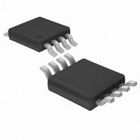
LTC2602CMS8#TR Linear Technology, LTC2602CMS8#TR Datasheet

LTC2602CMS8#TR
Specifications of LTC2602CMS8#TR
Available stocks
Related parts for LTC2602CMS8#TR
LTC2602CMS8#TR Summary of contents
Page 1
... During power-up, the voltage outputs rise less than 10mV above zero scale, and after power- up, they stay at zero scale until a valid write and update take place. , LTC and LT are registered trademarks of Linear Technology Corporation. All other trademarks are the property of their respective owners. 16-BIT V ...
Page 2
LTC2602/LTC2612/LTC2622 BSOLUTE (Note 1) Any Pin to GND ........................................... – 0. Any Pin ........................................................ Maximum Junction Temperature ......................... 125°C Operating Temperature Range LTC2602C/LTC2612C/LTC2622C .......... 0°C to 70°C LTC2602I/LTC2612I/LTC2622I ...
Page 3
ELECTRICAL C HARA TERISTICS C temperature range, otherwise specifications are at T SYMBOL PARAMETER PSRR Power Supply Rejection Ratio R DC Output Impedance OUT DC Crosstalk (Note 4) I Short-Circuit Output Current SC Reference Input Input Voltage Range Resistance Capacitance ...
Page 4
LTC2602/LTC2612/LTC2622 CHARACTERISTICS range, otherwise specifications are at T SYMBOL PARAMETER V = 2. SDI Valid to SCK Setup 1 t SDI Valid to SCK Hold 2 t SCK High Time 3 ...
Page 5
W U TYPICAL PERFOR A CE CHARACTERISTICS (LTC2602) DNL vs Temperature 1 0 4.096V REF 0.6 0.4 DNL (POS) 0.2 0 –0.2 DNL (NEG) –0.4 –0.6 –0.8 –1.0 –50 –30 – ...
Page 6
LTC2602/LTC2612/LTC2622 W U TYPICAL PERFOR A CE CHARACTERISTICS (LTC2622) Integral Nonlinearity (INL) 2 4.096V REF 1.5 1.0 0.5 0 –0.5 –1.0 –1.5 –2.0 0 1024 2048 3072 4095 CODE 2602 G31 (LTC2602/LTC2612/LTC2622) Current Limiting ...
Page 7
W U TYPICAL PERFOR A CE CHARACTERISTICS (LTC2602/LTC2612/LTC2622) Gain Error 0.4 0.3 0.2 0.1 0 –0.1 –0.2 –0.3 –0.4 2.5 3 3.5 4 4.5 5 5.5 V (V) CC 2602 G07 Midscale Glitch Impulse V OUT 10mV/DIV ...
Page 8
LTC2602/LTC2612/LTC2622 W U TYPICAL PERFOR A CE CHARACTERISTICS (LTC2602/LTC2612/LTC2622) Output Voltage Noise, 0.1Hz to 10Hz V OUT 10µV/DIV SECONDS 2602 G17 8 Short-Circuit Output Current vs V (Sinking) OUT 50 ...
Page 9
PIN FUNCTIONS CS/LD (Pin 1): Serial Interface Chip Select/Load Input. When CS/LD is low, SCK is enabled for shifting data on SDI into the register. When CS/LD is taken high, SCK is dis- abled and the specified ...
Page 10
LTC2602/LTC2612/LTC2622 U OPERATIO Power-On Reset The LTC2602/LTC2612/LTC2622 clear the outputs to zero scale when power is first applied, making system initializa- tion consistent and repeatable. For some applications, downstream circuits are active during DAC power-up, and may be sensitive to ...
Page 11
U OPERATIO INPUT WORD (LTC2602) COMMAND ADDRESS INPUT WORD (LTC2612) COMMAND ADDRESS INPUT WORD (LTC2622) COMMAND ADDRESS output pins ...
Page 12
LTC2602/LTC2612/LTC2622 U OPERATIO Board Layout The excellent load regulation and DC crosstalk perfor- mance of these devices is achieved in part by keeping “signal” and “power” grounds separated internally and by reducing shared internal resistance. The GND pin functions both ...
Page 13
U OPERATIO LTC2602/LTC2612/LTC2622 2602fa 13 ...
Page 14
LTC2602/LTC2612/LTC2622 U OPERATIO OUTPUT VOLTAGE 0V NEGATIVE INPUT CODE OFFSET (b) Figure 3. Effects of Rail-to-Rail Operation On a DAC Transfer Curve. (a) Overall Transfer Function (b) Effect of Negative Offset for Codes Near Zero Scale (c) Effect of Positive ...
Page 15
... LEAD COPLANARITY (BOTTOM OF LEADS AFTER FORMING) SHALL BE 0.102mm (.004") MAX Information furnished by Linear Technology Corporation is believed to be accurate and reliable. However, no responsibility is assumed for its use. Linear Technology Corporation makes no represen- tation that the interconnection of its circuits as described herein will not infringe on existing patent rights. ...
Page 16
... Rail-to-Rail Output www.linear.com ● = 4.5V to 5.5V 4.096V CC OUT = 2.7V to 5.5V 2.5V CC OUT = 5V(3V), Low Power, Deglitched CC OUT = 2.7V to 5.5V, Micropower, Rail-to-Rail Output CC = 2.7V to 5.5V, 60µA per DAC, Rail-to-Rail Output CC RD/LT 1205 REV A • PRINTED IN THE USA © LINEAR TECHNOLOGY CORPORATION 2003 2602fa ...


