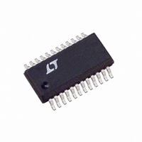
LTC1599AIG Linear Technology, LTC1599AIG Datasheet

LTC1599AIG
Specifications of LTC1599AIG
Related parts for LTC1599AIG
LTC1599AIG Summary of contents
Page 1
... CLVL pin logic low and to midscale when the CLVL pin logic high. For a full 16-bit wide parallel interface current output DAC, refer to the LTC1597 data sheet. For serial interface 16-bit current output DACs, refer to the LTC1595/LTC1596 data sheet. , LTC and LT are registered trademarks of Linear Technology Corporation. 5V 0.1µ ...
Page 2
... MIN MAX = 25°C (Note 5) A ● MIN MAX ● ±10 INFORMATION ORDER PART TOP VIEW NUMBER 1 24 CLR LTC1599ACG LTC1599BCG LTC1599AIG DGND LTC1599BIG LTC1599ACN LTC1599BCN LTC1599AIN LTC1599BIN 12 MLBYTE 13 N PACKAGE 24-LEAD PDIP = 125°C, θ = 95° 125°C, θ = 58°C/ W (N) ...
Page 3
ELECTRICAL CHARACTERISTICS temperature range, otherwise specifications are unless otherwise noted. A MIN MAX SYMBOL PARAMETER Reference Input R DAC Input Resistance (Unipolar) REF R1, R2 R1, R2 Resistance (Bipolar Feedback ...
Page 4
LTC1599 W U TYPICAL PERFOR A CE CHARACTERISTICS Midscale Glitch Impulse 40 USING AN LT1468 C = 30pF 30 FEEDBACK V = 10V REF 1.5nV-s TYPICAL –10 –20 – 30 – 0.2 0.4 0.6 0.8 ...
Page 5
W U TYPICAL PERFOR A CE CHARACTERISTICS Integral Nonlinearity vs Reference Voltage in Unipolar Mode 1.0 0.8 0.6 0.4 0.2 0 – 0.2 – 0.4 – 0.6 – 0.8 –1.0 –10 – 8 – 6 – 4 – ...
Page 6
LTC1599 W U TYPICAL PERFOR A CE CHARACTERISTICS Differential Nonlinearity vs Supply Voltage in Bipolar Mode 1.0 0.8 0.6 0.4 0 2.5V REF V – 0 2.5V REF – 0.4 – 0.6 – 0.8 ...
Page 7
PIN FUNCTIONS REF (Pin 1): Reference Input. Typically ±10V, accepts up to ±25V. In 2-quadrant mode, this pin is the reference input. In 4-quadrant mode, this pin is driven by external inverting reference amplifier. R2 (Pin 2): ...
Page 8
LTC1599 W BLOCK DIAGRA REF 48k 48k 12k R 3 COM 12k MSB ENABLE WR 12 BYTE ENABLE LSB ENABLE LOGIC MLBYTE ...
Page 9
U U APPLICATIONS INFORMATION Description The LTC1599 is a 16-bit multiplying, current output DAC with a 2-byte (8-bit wide) digital interface. The device operates from a single 5V supply and provides both unipolar 0V to – 10V ...
Page 10
LTC1599 U U APPLICATIONS INFORMATION configured in unipolar or bipolar modes of operation (Figures 1 and 3). These are the changes the op amp can cause to the INL, DNL, unipolar offset, unipolar gain error, bipolar zero and bipolar gain ...
Page 11
U U APPLICATIONS INFORMATION V REF DATA INPUTS LTC1599 MLBYTE MLBYTE LD WR CLR CLVL CLR CLVL Figure 1. Unipolar Operation (2-Quadrant ...
Page 12
LTC1599 U U APPLICATIONS INFORMATION V REF COM R1 8 DATA INPUTS MLBYTE MLBYTE WR LD CLR CLVL CLR CLVL Figure 3. Bipolar ...
Page 13
U U APPLICATIONS INFORMATION or 10V full-scale systems. However, as the circuit band- widths increase, filtering the output of the reference may be required to minimize output noise. Table 5. Partial List of LTC Precision References Recommended for Use with ...
Page 14
LTC1599 U U APPLICATIONS INFORMATION The output current of the DAC is converted to a voltage via U3 (LT1112), producing 0V to – 2.5V at Pin 1 of U3. The resulting current determined by two elements of ...
Page 15
U U APPLICATIONS INFORMATION A 16-Bit General Purpose Analog Output Circuit Industrial applications often use analog signals 5V 10V, ±5V or ±10V. The topology in Figure 6 uses an LTC1599 to produce a universal analog ...
Page 16
LTC1599 U U APPLICATIONS INFORMATION sn1599 1599fs ...
Page 17
U U APPLICATIONS INFORMATION Interfacing to the 68HC11 The circuit in Figure example of using the 68HC11 to control the LTC1599. Data is sent to the DAC using two 8-bit parallel transfers from the controller’s Port B. ...
Page 18
LTC1599 U U APPLICATIONS INFORMATION GETDATA PSHX PSHY PSHA LDY #$1000 Setup index * ***************************************** * Retrieve DAC data from memory and * send it to the LTC1599 ***************************************** * LDAA LBYTE BCLR PORTA,Y %00010000 * BCLR PORTA,Y %00001000 STAA ...
Page 19
... FLASH SHALL NOT EXCEED 0.254mm (0.010") PER SIDE Information furnished by Linear Technology Corporation is believed to be accurate and reliable. However, no responsibility is assumed for its use. Linear Technology Corporation makes no represen- tation that the interconnection of its circuits as described herein will not infringe on existing patent rights. ...
Page 20
... DAC LT1468 OUT2F + I 9 OUT2S 1596 TA03 1.265* (32.131) MAX DAC, ±4.5V Output Swing OUT DAC in MSOP. Output Swings from GND to REF. OUT 1599f LT/TP 1199 4K • PRINTED IN USA © LINEAR TECHNOLOGY CORPORATION 1999 V OUT N24 1098 sn1599 1599fs ...


