AD7302BR Analog Devices Inc, AD7302BR Datasheet
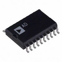
IC DAC 8BIT DUAL 2.7V 20-SOIC

AD7302BR

Manufacturer Part Number
AD7302BR
Description
IC DAC 8BIT DUAL 2.7V 20-SOIC
Manufacturer
Analog Devices Inc
Datasheet

Specifications of AD7302BR

Mounting Type
Surface Mount
Rohs Status
RoHS non-compliant
Settling Time
1.2µs
Number Of Bits
8
Data Interface
Parallel
Number Of Converters
2
Voltage Supply Source
Single Supply
Power Dissipation (max)
24.8mW
Operating Temperature
-40°C ~ 105°C
Package / Case
20-SOIC (7.5mm Width)
Resolution (bits)
8bit
No. Of Pins
20
Update Rate
0.833MSPS
Peak Reflow Compatible (260 C)
No
Supply Voltage
5.5V
No. Of Bits
8 Bit
Leaded Process Compatible
No
Lead Free Status / RoHS Status
Contains lead / RoHS non-compliant

Available stocks

Company
Part Number
Manufacturer
Quantity
Price
Part Number:
AD7302BR
Manufacturer:
ADI/亚德诺
Quantity:
20 000
Part Number:
AD7302BRU
Manufacturer:
AD
Quantity:
4 130
Part Number:
AD7302BRUZ
Manufacturer:
ADI/亚德诺
Quantity:
20 000
Part Number:
AD7302BRUZ-REEL7
Quantity:
17
Company:
Part Number:
AD7302BRUZ-REEL7
Quantity:
1 000
Part Number:
AD7302BRZ
Manufacturer:
Maxim
Quantity:
25
Part Number:
AD7302BRZ
Manufacturer:
ADI/亚德诺
Quantity:
20 000
Part Number:
AD7302BRZ-REEL
Manufacturer:
ADI/亚德诺
Quantity:
20 000
a
GENERAL DESCRIPTION
The AD7302 is a dual, 8-bit voltage out DAC that operates
from a single +2.7 V to +5.5 V supply. Its on-chip precision
output buffers allow the DAC outputs to swing rail to rail. The
AD7302 has a parallel microprocessor and DSP-compatible
interface with high speed registers and double buffered interface
logic. Data is loaded to the registers on the rising edge of CS or
WR and the A/B pin selects either DAC A or DAC B.
Reference selection for AD7302 can be either an internal
reference derived from the V
at the REFIN pin. Both DACs can be simultaneously updated
using the asynchronous LDAC input and can be cleared by
using the asynchronous CLR input.
The low power consumption of this part makes it ideally suited
to portable battery operated equipment. The power consump-
tion is less than 10 mW at 3.3 V, reducing to 3 W in power-
down mode.
The AD7302 is available in a 20-pin plastic dual-in-line package,
20-lead SOIC and a 20-lead TSSOP package.
REV. 0
Information furnished by Analog Devices is believed to be accurate and
reliable. However, no responsibility is assumed by Analog Devices for its
use, nor for any infringements of patents or other rights of third parties
which may result from its use. No license is granted by implication or
otherwise under any patent or patent rights of Analog Devices.
FEATURES
Two 8-Bit DACs In One Package
20-Lead DIP/SOIC/TSSOP Package
+2.7 V to +5.5 V Operation
Internal and External Reference Capability
DAC Power-Down Function
Parallel Interface
On-Chip Output Buffer
Low Power Operation 3 mA max @ 3.3 V
Power-Down to 1 A max @ 25 C
APPLICATIONS
Portable Battery Powered Instruments
Digital Gain and Offset Adjustment
Programmable Voltage and Current Sources
Programmable Attenuators
Rail-to-Rail Operation
DD
or an external reference applied
PRODUCT HIGHLIGHTS
1. Low Power, Single Supply Operation. This part operates
2. The on-chip output buffer amplifiers allow the outputs of the
3. Internal or external reference capability.
4. High speed parallel interface.
5. Power-Down Capability. When powered down the DAC
6. Packaged in 20-lead DIP, SOIC and TSSOP packages.
One Technology Way, P.O. Box 9106, Norwood, MA 02062-9106, U.S.A.
Tel: 617/329-4700
Fax: 617/326-8703
from a single +2.7 V to +5.5 V supply and typically consumes
15 mW at 5 V, making it ideal for battery powered applications.
DACs to swing rail to rail with a settling time of typically 1.2 s.
consumes less than 1 A at 25 C.
A/B
WR
Dual Voltage Output 8-Bit DAC
D7
CS
D0
2.7 V to 5.5 V, Parallel Input
FUNCTIONAL BLOCK DIAGRAM
PD
REGISTER
REGISTER
CONTROL
INPUT
INPUT
LOGIC
CLR
AD7302
World Wide Web Site: http://www.analog.com
REGISTER
REGISTER
LDAC
DAC
DAC
REFIN
I DAC A
I DAC B
© Analog Devices, Inc., 1997
MUX
V
AD7302
DD
2
POWER ON
RESET
I/V
I/V
DGND
V
V
AGND
OUT
OUT
A
B

Related parts for AD7302BR

AD7302BR Summary of contents

Page 1

FEATURES Two 8-Bit DACs In One Package 20-Lead DIP/SOIC/TSSOP Package +2 +5.5 V Operation Internal and External Reference Capability DAC Power-Down Function Parallel Interface On-Chip Output Buffer Rail-to-Rail Operation Low Power Operation 3 mA max @ 3.3 ...

Page 2

AD7302–SPECIFICATIONS Parameter STATIC PERFORMANCE Resolution Relative Accuracy Differential Nonlinearity Full-Scale Error Zero Code Error @ Gain Error Zero Code Temperature Coefficient DAC REFERENCE INPUT REFIN Input Range REFIN Input Impedance OUTPUT CHARACTERISTICS Output Voltage Range Output Voltage ...

Page 3

TIMING CHARACTERISTICS Limit at T Parameter (B Version 4 NOTES 1 ...

Page 4

... Therefore, proper ESD precautions are recommended to avoid performance degradation or loss of functionality. Model AD7302BN AD7302BR AD7302BRU *N = Plastic DIP Small Outline; RU =Thin Shrink Small Outline. TSSOP Package, Power Dissipation . . . . . . . . . . . . . 700 mW Thermal Impedance . . . . . . . . . . . . . . . . . . . . 143 C/W JA Lead Temperature, Soldering Vapor Phase (60 sec) ...

Page 5

Pin No. Mnemonic Function Parallel Data Inputs. Eight-bit data is loaded to the input register of the AD7302 under the control of CS 1-8 D7–D0 and WR Chip Select. Active low logic input. WR Write Input ...

Page 6

AD7302 TERMINOLOGY INTEGRAL NONLINEARITY For the DACs, relative accuracy or endpoint nonlinearity is a measure of the maximum deviation, in LSBs, from a straight line passing through the endpoints of the DAC transfer function. A graphical representation of the transfer ...

Page 7

AND 3V 720 DD INTERNAL REFERENCE 640 DAC LOADED WITH 00HEX 560 480 400 320 240 160 SINK CURRENT – mA Figure 2. Output Sink ...

Page 8

AD7302 CH1 M20.0ms 5.00V CH2 5.00V CH1 CH3 5.00V Figure 11. Power-On—RESET 0 0.4 INTERNAL REFERENCE 5k 100pf. LOAD 0.3 LIMITED CODE ...

Page 9

GENERAL DESCRIPTION D/A Section The AD7302 is a dual 8-bit voltage output digital-to-analog converter. The architecture consists of a reference amplifier, a current source DAC followed by a current-to-voltage converter capable of generating rail-to-rail voltages on the output of the ...

Page 10

AD7302 Automatic Update Mode In this mode of operation the LDAC signal is permanently tied low. The state of the LDAC is sampled on the rising edge of WR. LDAC being low allows the selected DAC register to be automatically ...

Page 11

V is the voltage applied to the external REFIN pin when REF the external reference is selected and is V internal reference is used. Table I. Output Voltage for Selected Input Codes Digital Input MSB . . . LSB Analog ...

Page 12

AD7302 MICROPROCESSOR INTERFACING AD7302–ADSP-2101/ADSP-2103 Interface Figure 29 shows an interface between the AD7302 and the ADSP-2101/ADSP-2103. The fast interface timing associated with the AD7302 allows easy interface to the ADSP-2101/ ADSP-2103. DMA14 ADDRESS BUS DMA0 A** ADDR DMS EN DECODE ...

Page 13

APPLICATIONS Bipolar Operation Using the AD7302 The AD7302 has been designed for single supply operation, but bipolar operation is achievable using the circuit shown in Figure 32. The circuit shown has been configured to achieve an output voltage range of ...

Page 14

AD7302 Programmable Current Source Figure 35 shows the AD7302 used as the control element of a programmable current source. In this circuit the full-scale current is set to 1 mA. The output voltage from the DAC is applied across the ...

Page 15

SEATING REV. 0 OUTLINE DIMENSIONS Dimensions shown in inches and (mm). 20-Lead Plastic DIP (N-20) 1.060 (26.90) 0.925 (23.50 0.280 (7.11) 0.240 (6.10) 1 ...

Page 16

–16– ...

Related keywords