DAC10GS Analog Devices Inc, DAC10GS Datasheet - Page 9
DAC10GS
Manufacturer Part Number
DAC10GS
Description
IC DAC 10BIT MULT HS 85NS 18SOIC
Manufacturer
Analog Devices Inc
Datasheet
1.DAC10GSZ-REEL.pdf
(10 pages)
Specifications of DAC10GS
Rohs Status
RoHS non-compliant
Settling Time
85ns
Number Of Bits
10
Data Interface
Parallel
Number Of Converters
1
Voltage Supply Source
Dual ±
Power Dissipation (max)
285mW
Operating Temperature
0°C ~ 70°C
Mounting Type
Surface Mount
Package / Case
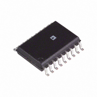
18-SOIC (7.5mm Width)
Available stocks
Company
Part Number
Manufacturer
Quantity
Price

Part Number:
DAC10GS
Manufacturer:
ADI/亚德诺
Quantity:
20 000
Company:
Part Number:
DAC10GSZ
Manufacturer:
Analog Devices Inc
Quantity:
135
Part Number:
DAC10GSZ
Manufacturer:
ADI/亚德诺
Quantity:
20 000


ANALOG OUTPUT CURRENTS
Both true and complemented output sink currents are provided
where I
when a “1” is applied to each logic input. As the binary count
increases, the sink current at Pin 4 increases proportionally, in
the fashion of a “positive logic” D/A converter. When a “0” is
applied to any input bit, that current is turned off at Pin 4 and
turned on at Pin 2. A decreasing logic count increases I
a negative or inverted logic D/A converter. Both outputs may be
used simultaneously. If one of the outputs is not required, it
must still be connected to ground or to a point capable of sourc-
ing I
Both outputs have an extremely wide voltage compliance en-
abling fast direct current-to-voltage conversion through a resis-
tor tied to ground or other voltage source. Positive compliance
is 36 V above V– and is independent of the positive supply.
Negative compliance is +10 V above V–.
The dual outputs enable double the usual peak-to-peak load
swing when driving loads in quasi-differential fashion. This
feature is especially useful in cable driving, CRT deflection and
in other balanced applications such as driving center-tapped
coils and transformers.
POWER SUPPLIES
The DAC10 operates over a wide range of power supply volt-
ages from a total supply of 9 V to 36 V. When operating with V–
supplies of –10 V or less, I
reference current operation decreases power consumption and
increases negative compliance, reference amplifier negative
common-mode range, negative logic input range and negative
logic threshold range; consult the various figures for guidance.
For example, operation at –9 V with I
mended because negative output compliance would be reduced
to near zero. Operation from lower supplies is possible, however
at least 8 V total must be applied to ensure turn-on of the inter-
nal bias network.
Symmetrical supplies are not required, as the DAC10 is quite
insensitive to variations in supply voltage. Battery operation is
feasible as no ground connection is required; however, an artifi-
cial ground may be used to ensure that logic swings, etc., remain
within acceptable limits.
TEMPERATURE PERFORMANCE
The nonlinearity and monotonicity specifications of the DAC10
are guaranteed to apply over the entire rated operating tempera-
ture range. Full-scale output current drift is tight, typically
+10 ppm/ C, with zero-scale output current and drift essentially
negligible compared to 1/2 LSB.
REV. D
FS
. DO NOT LEAVE AN UNUSED OUTPUT PIN OPEN.
O
I
O
I
FS
. Current appears at the “true” output
REF
1 mA is recommended. Low
REF
= 2 mA is not recom-
O
as in
–9–
The temperature coefficient of the reference resistor, R14,
should match and track that of the output resistor for minimum
overall full-scale drift. Settling times of the DAC10 decrease
approximately 10% at –55 C; an increase of about 15% is typi-
cal at +125 C.
SETTLING TIME
The DAC10 is capable of extremely fast settling times; typically
85 ns at I
layout must be employed to obtain full performance potential
during testing and application. The logic switch design enables
propagation delays of only 35 ns for each of the 10 bits. Settling
time to within 1/2 LSB of the LSB is therefore 35 ns, with each
progressively larger bit taking successively longer. The MSB
settles in 85 ns, thus determining the overall settling time of
130 ns. Settling to 8-bit accuracy requires about 60 ns to 78 ns.
The output capacitance of the DAC10, including the package, is
approximately 18 pF; therefore, the output RC time constant
dominates settling time if R
Settling time and propagation delay are relatively insensitive to
logic input amplitude and rise and fall times, due to the high
gain of the logic switches. Settling time also remains essentially
constant for I
for lower I
values lies in the ability to attain a given output level with lower
load resistors, thus reducing the output RC time constant.
Measurement of settling time requires the ability to accurately
resolve 2 A; therefore, a 4 k load is needed to provide ad-
equate drive for most oscilloscopes. The settling time fixture of
schematic titled “Settling Time Measurement” uses a cascode
design to permit driving a 4 k load with less than 5 pF of para-
sitic capacitance at the measurement node. At I
than 1 mA, excessive RC damping of the output is difficult to
prevent while maintaining adequate sensitivity. However, the
major carry from 0111111111 to 1000000000 provides an accu-
rate indicator of settling time. This code change does not re-
quire the normal 6.2 time constants to settle to within 0.2% of
the final value, and thus settling times may be observed at lower
values of I
DAC10 switching transients or “glitches” are very low and may
be further reduced by small capacitive loads at the output with a
minor sacrifice in settling time.
Fastest operation can be obtained by using short leads, minimiz-
ing output capacitance and load resistor values, and by adequate
bypassing at the supply, reference and V
do not require large electrolytic bypass capacitors as the supply
current drain is independent of input logic states; 0.1 F capaci-
tors at the supply pins provide full transient protection.
REF
REF
REF
= 2 mA. Judicious circuit design and careful board
.
REF
values. The principal advantage of higher I
values down to 1 mA, with gradual increases
L
> 500 .
LC
terminals. Supplies
REF
DAC10
values of less
REF
Related parts for DAC10GS
Image
Part Number
Description
Manufacturer
Datasheet
Request
R

Part Number:
Description:
±1.7g Dual-Axis IMEMS Accelerometer Evaluation Board
Manufacturer:
Analog Devices Inc
Datasheet:

Part Number:
Description:
Inertial Sensor Evaluation System
Manufacturer:
Analog Devices Inc
Datasheet:
Part Number:
Description:
Manufacturer:
Analog Devices Inc
Datasheet:
Part Number:
Description:
Manufacturer:
Analog Devices Inc
Datasheet:
Part Number:
Description:
Manufacturer:
Analog Devices Inc
Datasheet:
Part Number:
Description:
Manufacturer:
Analog Devices Inc
Datasheet:
Part Number:
Description:
Manufacturer:
Analog Devices Inc
Datasheet:
Part Number:
Description:
Manufacturer:
Analog Devices Inc
Datasheet:
Part Number:
Description:
Manufacturer:
Analog Devices Inc
Datasheet:
Part Number:
Description:
Manufacturer:
Analog Devices Inc
Datasheet:
Part Number:
Description:
Manufacturer:
Analog Devices Inc
Datasheet:
Part Number:
Description:
Manufacturer:
Analog Devices Inc
Datasheet:
Part Number:
Description:
Manufacturer:
Analog Devices Inc
Datasheet: