LM48511SQ National Semiconductor, LM48511SQ Datasheet
LM48511SQ
Specifications of LM48511SQ
Available stocks


Related parts for LM48511SQ

LM48511SQ Summary of contents
Page 1
... Superior click and pop suppression eliminates au- dible transients during power-up and shutdown. EMI Graph Boomer ® registered trademark of National Semiconductor Corporation. © 2008 National Semiconductor Corporation Key Specifications ■ Quiescent Power Supply Current V ...
Page 2
Typical Application FIGURE 2. Typical LM48511 Audio Amplifier Application Circuit www.national.com 2 300222i3 ...
Page 3
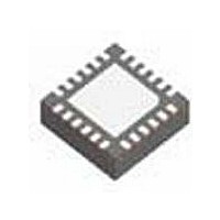
... Connection Diagrams SQ Package Top View Order Number LM48511SQ See NS Package Number SQA24B SQ Package Marking 300222d5 Top View U — Wafer fab code Z — Assembly plant XY — 2 Digit date code TT — Lot traceability 3 300222d4 www.national.com ...
Page 4
Pin Descriptions LLP-24 Pin 1 2 22,23 24 DAP www.national.com Name Regulator Feedback Select. Connect to VDD to select feedback FB_SEL network ...
Page 5
... Absolute Maximum Ratings If Military/Aerospace specified devices are required, please contact the National Semiconductor Sales Office/ Distributors for availability and specifications. Supply Voltage (V , PV1 Storage Temperature Input Voltage Power Dissipation (Note 3) ESD Susceptibility (Note 4) ESD Susceptibility (Note 5) Junction Temperature Electrical Characteristics V The following specifications apply for V 8Ω ...
Page 6
Symbol Parameter ε Output Noise OS Power Supply Rejection Ratio PSRR (Input Referred) Common Mode Rejection Ratio CMRR (Input Referred) η Efficiency V Feedback Pin Reference Voltage FB Electrical Characteristics V The following specifications apply for 1kHz, ...
Page 7
Symbol Parameter P Output Power O THD+N Total Harmonic Distortion + Noise ε Output Noise OS Power Supply Rejection Ratio PSRR (Input Referred) Common Mode Rejection Ratio CMRR (Input Referred) η Efficiency V Feedback Pin Reference Voltage FB Conditions = ...
Page 8
Electrical Characteristics V The following specifications apply for V 8Ω 1kHz, SS/FF = GND, unless otherwise specified. Limits apply for T Symbol Parameter I Quiescent Power Supply Current DD I Shutdown Current SD V Logic Voltage Input High ...
Page 9
Symbol Parameter Power Supply Rejection Ratio PSRR (Input Referred) Common Mode Rejection Ratio CMRR (Input Referred) η Efficiency V Feedback Pin Reference Voltage FB Note 1: “Absolute Maximum Ratings” indicate limits beyond which damage to the device may occur, including ...
Page 10
Typical Performance Characteristics THD+N vs Frequency 2W, filter = 22kHz THD+N vs Frequency 1.5W, filter = 22kHz THD+N vs Output ...
Page 11
THD+N vs Output Power = 8Ω 3V, 3.6V, 5V 1kHz, filter = 22kHz 4.87kΩ 300222i1 Boost Amplifier vs Output Power = 8Ω 5V ...
Page 12
PSRR vs Frequency V = 3.6V 200mV RIPPLE PP Supply Current vs Supply Voltage PV = 7.8V 1 Supply Current vs Supply Voltage PV = 4.8V 1 www.national.com = 8Ω ...
Page 13
Power Dissipation vs Output Power = 8Ω 3.6V 7V 300222f8 Boost Converter Efficiency vs I LOAD( 300222h8 Boost Converter Efficiency vs I LOAD(DC) ...
Page 14
Application Information GENERAL AMPLIFIER FUNCTION The LM48511 features a Class D audio power amplifier that utilizes a filterless modulation scheme, reducing external component count, conserving board space and reducing sys- tem cost. The outputs of the device transition from PV1 ...
Page 15
FB_SEL can be susceptible to noise interference. To prevent an accidental state change, either bypass FB_SEL with a 0.1µF capacitor to GND, or connect the higher voltage feed- back network to FB_GND0, and the lower voltage feedback network to FB_GND1. ...
Page 16
Selecting a soft-start capacitor (C SS off between the wake-up time and the startup transient cur- rent. Using a larger capacitor value will increase wake-up time and decrease startup transient current while the apposite ef- fect happens with a smaller ...
Page 17
Where R is the ESR of the output capacitor. The value given by: FB3 π CALCULATING REGULATOR OUTPUT CURRENT The load current of the boost converter is related to ...
Page 18
Build Of Materials Designator Description Cf1 CHIP CAPACITOR GENERIC CINA CHIP CAPACITOR GENERIC CINB CHIP CAPACITOR GENERIC Co CHIP CAPACITOR GENERIC Cs1 CHIP CAPACITOR GENERIC Cs2 CHIP CAPACITOR GENERIC D1 SCHOTTKY DIO L1 R1 CHIP RESISTOR GENERIC R2 CHIP RESISTOR ...
Page 19
Revision History Rev Date 1.0 07/24/07 1.1 07/25/07 1.2 09/25/07 1.3 11/06/07 1.4 02/25/08 Description Initial release. Input some text edits. Changed the Amplifier Voltage (Operating Ratings section) from 5.0V to 4.8V. Added another Po (@Vdd = 5V ...
Page 20
... Physical Dimensions www.national.com inches (millimeters) unless otherwise noted SQ Package Order Number LM48511SQ NS Package Number SQA24B 20 ...
Page 21
Notes 21 www.national.com ...
Page 22
... For more National Semiconductor product information and proven design tools, visit the following Web sites at: Products Amplifiers www.national.com/amplifiers Audio www.national.com/audio Clock Conditioners www.national.com/timing Data Converters www.national.com/adc Displays www.national.com/displays Ethernet www.national.com/ethernet Interface www.national.com/interface LVDS www.national.com/lvds Power Management www.national.com/power Switching Regulators www.national.com/switchers LDOs www ...