PRIXP425BC 869083 Intel, PRIXP425BC 869083 Datasheet - Page 127
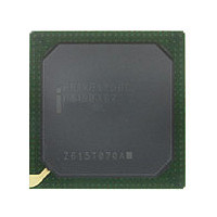
PRIXP425BC 869083
Manufacturer Part Number
PRIXP425BC 869083
Description
Manufacturer
Intel
Datasheet
1.PRIXP425BC_869083.pdf
(130 pages)
Specifications of PRIXP425BC 869083
Core Operating Frequency
400MHz
Package Type
BGA
Pin Count
492
Mounting
Surface Mount
Operating Temperature (max)
70C
Operating Temperature (min)
0C
Operating Temperature Classification
Commercial
Lead Free Status / Rohs Status
Compliant


Intel
Table 68.
5.6
August 2006
Document Number: 252479-006US
®
IXP42X product line and IXC1100 control plane processors
Reset Timings Table Parameters
Power Sequence
The 3.3-V I/O voltage (V
processor voltage (V
processors’ voltage (V
(V
V
1
There are no power-down requirements for the IXP42X product line and IXC1100
control plane processors.
T
T
T
T
T
T
Notes:
1.
2.
3.
RELEASE_PWRON_RST_N
RELEASE_RESET_IN_N
PLL_LOCK
EX_ADDR_SETUP
EX_ADDR_HOLD
WARM_RESET
CCOSCP
µ
CCP
s. The T
). The V
Symbol
T
The expansion bus address is captured as a derivative of the RESET_IN_N signal going high. When a
programmable-logic device is used to drive the EX_ADDR signals instead of pull-downs, the signals
must be active until PLL_LOCK goes high.
PLL_LOCK is deasserted immediately when watchdog timer event occurs, or when RESET_IN_N is
asserted, or when PWRON_RST_N is asserted. PLL_LOCK remains deasserted for ~24 ref_clocks after
the watchdog reset is deasserted (internal to the chip). A ref clock time period is 1/CLKIN.
RELEASE_PWRON_RST_N
follows the V
POWER_UP
CCOSC
Intel
, V
timing parameter is measured from V
Minimum time required to hold the
PWRON_RST_N at logic 0 state after
stable power has been applied to the
IXP42X product line and IXC1100 control
plane processors.
Minimum time required to hold the
RESET_IN_N at logic 0 state after
PWRON_RST_N has been released to a
logic 1 state. The RESET_IN_N signal
must be held low when the
PWRON_RST_N signal is held low.
Maximum time for PLL_LOCK signal to
drive to logic 1 after RESET_IN_N is
driven to logic 1 state. The boot
sequence does not occur until this period
is complete.
Minimum time for the EX_ADDR signals
to drive the inputs prior to RESET_IN_N
being driven to logic 1 state. This is used
for sampling configuration information.
Minimum/maximum time for the
EX_ADDR signals to drive the inputs prior
to PLL_LOCK being driven to logic 1
state. This is used for sampling
configuration information.
Minimum time required to drive
RESET_IN_N signal to logic 0 in order to
cause a Warm Reset in the IXP42X
product line and IXC1100 control plane
processors
supply must not be disturbed and
PWRON_RST_N signal must remain at
logic high during the entire process.
CC
CCP
CCPLL1
CC
®
). The IXP42X product line and IXC1100 control plane
IXP42X Product Line of Network Processors and IXC1100 Control Plane Processor
) must never become stable prior to the 3.3-V I/O voltage
is the time required for the internal oscillator to reach stability.
CCP
power-up pattern. The value for T
, and V
) must be powered up 1
.
During this period, the power
Parameter
CCPLL2
voltages follow the V
µs
2000
Min.
500
before the Intel XScale
10
50
0
CCP
POWER_UP
Typ.
at 3.3 V and V
CC
power-up pattern. The
Max.
10
20
must be at least
Units
CC
ns
ns
µs
ns
ns
ns
®
at 1.3 V.
Datasheet
Note
1
2
2
127
Related parts for PRIXP425BC 869083
Image
Part Number
Description
Manufacturer
Datasheet
Request
R

Part Number:
Description:
IC NETWRK PROCESSR 400MHZ 492BGA
Manufacturer:
Intel
Datasheet:

Part Number:
Description:
Microprocessor: Intel Celeron M Processor 320 and Ultra Low Voltage Intel Celeron M Processor at 600MHz
Manufacturer:
Intel Corporation
Part Number:
Description:
Intel 82550 Fast Ethernet Multifunction PCI/CardBus Controller
Manufacturer:
Intel Corporation
Datasheet:
Part Number:
Description:
Intel StrataFlash memory 32 Mbit. Access speed 120 ns
Manufacturer:
Intel Corporation
Datasheet:
Part Number:
Description:
Intel StrataFlash memory 32 Mbit. Access speed 120 ns
Manufacturer:
Intel Corporation
Datasheet:
Part Number:
Description:
Intel StrataFlash memory 64 Mbit. Access speed 150 ns
Manufacturer:
Intel Corporation
Datasheet:
Part Number:
Description:
Intel StrataFlash memory 32 Mbit. Access speed 100 ns
Manufacturer:
Intel Corporation
Datasheet:
Part Number:
Description:
DA28F640J5A-1505 Volt Intel StrataFlash Memory
Manufacturer:
Intel Corporation
Datasheet:
Part Number:
Description:
5 Volt Intel StrataFlash?? Memory
Manufacturer:
Intel Corporation
Datasheet:
Part Number:
Description:
5 Volt Intel StrataFlash?? Memory
Manufacturer:
Intel Corporation
Part Number:
Description:
Intel 6300ESB I/O Controller Hub
Manufacturer:
Intel Corporation
Datasheet:
Part Number:
Description:
Intel 82801DB I/O Controller Hub (ICH4), Pb-Free SLI
Manufacturer:
Intel Corporation
Datasheet:
Part Number:
Description:
Intel 82801FB I/O Controller Hub (ICH6)
Manufacturer:
Intel Corporation
Datasheet:
Part Number:
Description:
Intel Strataflash Memory28F128J3 28F640J3 28F320J3
Manufacturer:
Intel Corporation
Datasheet: