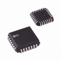
AD7846JP Analog Devices Inc, AD7846JP Datasheet

AD7846JP
Specifications of AD7846JP
Available stocks
Related parts for AD7846JP
AD7846JP Summary of contents
Page 1
FEATURES 16-bit monotonicity over temperature ±2 LSBs integral linearity error Microprocessor compatible with readback capability Unipolar or bipolar output Multiplying capability Low power (100 mW typical) GENERAL DESCRIPTION The AD7846 is a 16-bit DAC constructed with the Analog Devices, 2 ...
Page 2
AD7846 TABLE OF CONTENTS Features .............................................................................................. 1 Functional Block Diagram .............................................................. 1 General Description ......................................................................... 1 Product Highlights ........................................................................... 1 Revision History ............................................................................... 2 Specifications ..................................................................................... 3 AC Performance Characteristics ................................................ 4 Timing Characteristics ................................................................ 5 Absolute Maximum Ratings ............................................................ ...
Page 3
SPECIFICATIONS V = +14. +15. −14. –15. connected All specifications T IN Table 1. Parameter 1 RESOLUTION UNIPOLAR OUTPUT Relative Accuracy at +25° ...
Page 4
AD7846 Parameter 1 DIGITAL OUTPUTS V (Output Low Voltage (Output High Voltage) OH Floating State Leakage Current Floating State Output Capacitance 2 3 POWER REQUIREMENTS ...
Page 5
TIMING CHARACTERISTICS V = +14. +15. −14. −15. Table 3. 1 Parameter Limit MIN MAX ...
Page 6
AD7846 ABSOLUTE MAXIMUM RATINGS Table 4. Parameter Rating V to DGND −0 + DGND −0 (whichever is lower DGND +0 − DGND V ...
Page 7
PIN CONFIGURATIONS AND FUNCTION DESCRIPTIONS DB2 1 28 DB1 2 27 DB0 OUT AD7846 REF+ TOP VIEW (Not to Scale REF– ...
Page 8
AD7846 TYPICAL PERFORMANCE CHARACTERISTICS A1 –0.40V 1V 2mV 20µs Figure 9. AC Feedthrough rms, 10 kHz Sine Wave REF +15V –15V +1V rms REF + V ...
Page 9
±5V REF + V , ±10V OUT + 10V 5V 2µs Figure 15. Pulse Response (Large Signal) A1 0.025V V , ±50mV REF + V , ±100mV OUT + 100mV 50mV 1µs Figure 16. Pulse Response ...
Page 10
AD7846 TERMINOLOGY Least Significant Bit This is the analog weighting of 1 bit of the digital word in a DAC. For the AD7846, 1 LSB = (V − V REF+ Relative Accuracy Relative accuracy or endpoint nonlinearity is a measure ...
Page 11
CIRCUIT DESCRIPTION DIGITAL SECTION Figure 20 shows the digital control logic and on-chip data latches in the AD7846. Table 7 is the associated truth table. The digital- to-analog converter (DAC) has two latches that are controlled by four signals: CS ...
Page 12
AD7846 V REF+ DAC1 S1 S3 S15 S17 DB15 TO DB12 V REF– OUTPUT STAGE The output stage of the AD7846 is shown in Figure 22 capable of driving a 2 kΩ/1000 pF load. It also has a ...
Page 13
UNIPOLAR BINARY OPERATION Figure 23 shows the AD7846 in the unipolar binary circuit configuration. The DAC is driven by the AD586 Because R is tied the output amplifier has a gain and the output ...
Page 14
AD7846 BIPOLAR OPERATION Figure 24 shows the AD7846 set up for ±10 V bipolar operation. The AD588 provides precision ±5 V tracking outputs that are fed to the V and V inputs of the AD7846. The code table REF+ REF− ...
Page 15
POSITION MEASUREMENT APPLICATION Figure 25 shows the AD7846 in a position measurement applica- tion using an linear variable displacement transducer (LVDT), an AD630 synchronous demodulator and a comparator to make a 16-bit LVDT-to-digital converter. The LVDT is excited with a ...
Page 16
AD7846 MICROPROCESSOR INTERFACING AD7846-TO-8086 INTERFACE Figure 26 shows the 8086 16-bit processor interfacing to the AD7846. The double buffering feature of the DAC is not used in this circuit because LDAC is permanently tied AD0 to AD15 ...
Page 17
DIGITAL FEEDTHROUGH In the preceding interface configurations, most digital inputs to the AD7846 are directly connected to the microprocessor bus. Even when the device is not selected, these inputs are constantly changing. The high frequency logic activity on the bus ...
Page 18
AD7846 APPLICATION HINTS NOISE In high resolution systems, noise is often the limiting factor. With span, a 16-bit LSB is 152 μV (–96 dB). Thus, the noise floor must stay below − the frequency range ...
Page 19
C1 10µF R1 39kΩ C2 0.1µ C12 1µ AD588 100kΩ –15V 0.1µ 100kΩ V OUT (+10V TO –10V) +15V C5 C6 ...
Page 20
AD7846 OUTLINE DIMENSIONS PIN 1 0.225(5.72) MAX 0.200 (5.08) 0.125 (3.18) 0.026 (0.66) 0.014 (0.36 0.250 (6.35) MAX 0.200 (5.08) 0.115 (2.92) 0.022 (0.56) 0.014 (0.36) 0.100 (2.54) 0.005 (0.13) MAX MIN 28 15 0.610 (15.49) 0.500 (12.70) ...
Page 21
SQ MAX 0.442 (11.23) SQ 0.088 (2.24) 0.054 (1.37) CONTROLLING DIMENSIONS ARE IN INCHES; MILLIMETER DIMENSIONS (IN PARENTHESES) ARE ROUNDED-OFF INCH EQUIVALENTS FOR REFERENCE ONLY AND ARE NOT APPROPRIATE FOR USE IN ...
Page 22
... AD7846KN 0°C to +70°C AD7846KNZ 0°C to +70°C AD7846JP 0°C to +70°C AD7846JP-REEL 0°C to +70°C AD7846JPZ 0°C to +70°C AD7846JPZ-REEL 0°C to +70°C AD7846KP 0°C to +70°C AD7846KP-REEL 0°C to +70°C AD7846KPZ 0°C to +70°C AD7846KPZ-REEL 0°C to +70°C AD7846AP − ...
Page 23
NOTES Rev Page AD7846 ...
Page 24
AD7846 NOTES ©2000–2010 Analog Devices, Inc. All rights reserved. Trademarks and registered trademarks are the property of their respective owners. D08490-0-4/10(G) Rev Page ...


