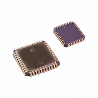
AD664BJ Analog Devices Inc, AD664BJ Datasheet - Page 17

AD664BJ
Manufacturer Part Number
AD664BJ
Description
IC DAC 12BIT QUAD MONO 44-JLCC
Manufacturer
Analog Devices Inc
Datasheet
1.AD664JNZ-BIP.pdf
(20 pages)
Specifications of AD664BJ
Rohs Status
RoHS non-compliant
Settling Time
8µs
Number Of Bits
12
Data Interface
Parallel
Number Of Converters
4
Voltage Supply Source
Dual ±
Power Dissipation (max)
525mW
Operating Temperature
-40°C ~ 85°C
Mounting Type
Surface Mount
Package / Case
44-JLCC
Number Of Channels
4
Resolution
12b
Conversion Rate
125KSPS
Interface Type
Parallel
Single Supply Voltage (typ)
Not RequiredV
Dual Supply Voltage (typ)
±15V
Architecture
R-2R
Power Supply Requirement
Dual
Output Type
Voltage
Integral Nonlinearity Error
±0.75LSB
Single Supply Voltage (min)
Not RequiredV
Single Supply Voltage (max)
Not RequiredV
Dual Supply Voltage (min)
±11.4V
Dual Supply Voltage (max)
±16.5V
Operating Temp Range
-40C to 85C
Operating Temperature Classification
Industrial
Mounting
Surface Mount
Pin Count
44
Package Type
JLCC
Lead Free Status / Rohs Status
Compliant
Available stocks
Company
Part Number
Manufacturer
Quantity
Price
REV. C
The following IBM PC Basic routine produces four output volt-
age ramps from one AD664. Line numbers 10 through 70 de-
fine the hardware addresses for the first and second ranks of
DAC registers as well as the first and second ranks of the mode
select register. Program variables are initialized in line numbers
110 through 130. Line number 170 writes “0s” out to the first
rank and, then, the second rank of the mode select register.
5
10
20
30
40
50
60
70
80
90
100
110
120
130
140
150
160
170
180
190
200
210
220
230
240
250
260
270
280
290
300
310
320
330
340
400
410
420
430
440
450
500
510
520
530
REM----AD664 LISSAJOUS PATTERNS----
REM ---ASSIGN HARDWARE ADDRESSES---
DACA = 785
DACB = 787
DACC = 789
DACD = 791
DAC2ND = 792
MODE1 = 769: MODE2 = 776
REM
REM
REM ---INITIALIZE VARIABLES---
X = 0: Y1 = 128: Y2 = 64: Y3 = 32
CX = 1: CY1 = 1: CY2 = -1: CY3= 1
FX = 9: FY1 = 5: FY2 = 13: FY3 = 15
REM
REM
REM ---INITIALIZE MODES AND GAINS---
OUT MODE1,0: OUT MODE2,0
REM
REM
REM ---CALCULATE VARIABLES---
X = X + FX*CX
Y1 = Y1 + FY1*CY1
Y2 = Y2 + FY2*CY2
Y3 = Y3 + FY3*CY3
IF X > 255 THEN X = 255: CX = -1: GOTO 270
IF X < 0 THEN X = 0: CX = 1
IF Y1 > 255 THEN Y1 = 255: CY1 = -1: GOTO 290
IF Y1 < 0 THEN Y1 = 0: CY1 = 1
IF Y2 > 255 THEN Y2 = 255: CY2 = -1 GOTO 310
IF Y2 < 0 THEN Y2 = 0: CY2 = -1
IF Y3 > 255 THEN Y3 = 255: CY3 = -1: GOTO 400
IF Y3 < 0 THEN Y3 = 0: CY3 = 1
REM
REM
REM ---SEND DAC DATA---
OUT DACA,X
OUT DACB,Yl
OUT DACC,Y2
OUT DACD,Y3
OUT DAC2ND,0
REM
REM
REM ---LOOP BACK---
GOTO 210
–17–
Line numbers 200 through 320 calculate output voltages. Fi-
nally line numbers 410 through 450 update the first, then the
second ranks of the DAC input registers. Hardware registers
may be read with the “INP” instruction. For example, the con-
tents of the DAC A register may be accessed with the following
com mand: Line# A = INP(DACA).
AD664


