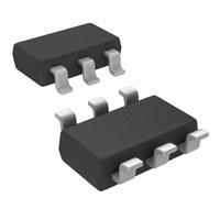
DAC121C081CIMKX/NOPB National Semiconductor, DAC121C081CIMKX/NOPB Datasheet - Page 18

DAC121C081CIMKX/NOPB
Manufacturer Part Number
DAC121C081CIMKX/NOPB
Description
DAC 12BIT MICROPWR I2C TSOT23-6
Manufacturer
National Semiconductor
Series
PowerWise®r
Datasheet
1.DAC121C081CISDNOPB.pdf
(24 pages)
Specifications of DAC121C081CIMKX/NOPB
Settling Time
6µs
Number Of Bits
12
Data Interface
I²C
Number Of Converters
1
Voltage Supply Source
Single Supply
Power Dissipation (max)
730µW
Operating Temperature
-40°C ~ 125°C
Mounting Type
Surface Mount
Package / Case
TSOT-23-6, TSOT-6
For Use With
DAC121C08XEB - BOARD EVAL FOR DAC121C081/5
Lead Free Status / RoHS Status
Lead free / RoHS Compliant
Other names
DAC121C081CIMKX
www.national.com
1.5 DAC REGISTER
The DAC register, Figure 8, has sixteen bits. The first two bits
are always zero. The next two bits determine the mode of
operation (normal mode or one of three power-down modes).
The final twelve bits of the shift register are the data bits. The
data format is straight binary (MSB first, LSB last), with twelve
0's corresponding to an output of 0V and twelve 1's corre-
sponding to a full-scale output of V
the DAC Register, V
ACK following the lower data byte.
1.6 POWER-ON RESET
The power-on reset circuit controls the output voltage of the
DAC during power-up. Upon application of power, the DAC
register is filled with zeros and the output voltage is 0 Volts.
The output remains at 0V until a valid write sequence is made
to the DAC.
When resetting the device, it is crutial that the V
lowered to a maximum of 200mV before the supply is raised
again to power-up the device. Dropping the supply to within
200mV of GND during a reset will ensure the ADC performs
as specified.
1.7 SIMULTANEOUS RESET
The broadcast address allows the I
word to multiple DACs simultaneously. Provided that all of the
DACs exist on a single I
the broadcast address is used to address the bus. This fea-
ture allows the master to reset all of the DACs on a shared
I
writes a power-down code to the bus with the broadcast ad-
dress, all of the DACs will power-down simultaneously.
2
C bus to a specific digital code. For instance, if the master
FIGURE 8. DAC Register Contents
OUT
2
will update on the rising edge of the
C bus, every DAC will update when
A
2
C master to write a single
- 1 LSB. When writing to
A
supply be
30004908
18
1.8 POWER-DOWN MODES
The DAC121C081 has three power-down modes. In power-
down mode, the supply current drops to 0.13µA at 3V and
0.15µA at 5V (typ). The DAC121C081 is put into power-down
mode by writing a one to PD1 and/or PD0. The outputs can
be set to high impedance, terminated by 2.5 kΩ to GND, or
terminated by 100 kΩ to GND (see Figure 8).
The bias generator, output amplifier, resistor string, and other
linear circuitry are all shut down in any of the power-down
modes. When the DAC121C081 is powered down, the value
written to the DAC register, including the power-down bits, is
saved. While the DAC is in power-down, the saved DAC reg-
ister contents can be read back. When the DAC is brought out
of power-down mode, the DAC register contents will be over-
written and V
value.
The time to exit power-down (Wake-Up Time) is typically
0.8µsec at 3V and 0.5µsec at 5V.
1.9 ADDITIONAL TIMING INFORMATION: t
The t
bus. After the SCL bus is driven low by the I
SDA bus will be held for a short time by the DAC121C081.
This time is referred to as t
the relationship between the fall of SCL, at the 30% threshold,
to the time when the DAC begins to transition the SDA bus.
The t
of the SDA bus. The DAC is only in control of the bus during
an ACK by the DAC121C081 or a data byte read from the
DAC (see Figure 7).
The t
Mode and 38nsec in Hs-Mode.
outz
outz
outz
specification only applies when the DAC is in control
specification is provided to aid the design of the I
specification is typically 87nsec in Standard-Fast
FIGURE 9. Data Output Timing
OUT
will be updated with the new 12-bit data
outz
. The following figure illustrates
30004965
outz
2
C master, the
2
C


