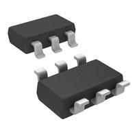
DAC121C081CIMKX/NOPB National Semiconductor, DAC121C081CIMKX/NOPB Datasheet - Page 21

DAC121C081CIMKX/NOPB
Manufacturer Part Number
DAC121C081CIMKX/NOPB
Description
DAC 12BIT MICROPWR I2C TSOT23-6
Manufacturer
National Semiconductor
Series
PowerWise®r
Datasheet
1.DAC121C081CISDNOPB.pdf
(24 pages)
Specifications of DAC121C081CIMKX/NOPB
Settling Time
6µs
Number Of Bits
12
Data Interface
I²C
Number Of Converters
1
Voltage Supply Source
Single Supply
Power Dissipation (max)
730µW
Operating Temperature
-40°C ~ 125°C
Mounting Type
Surface Mount
Package / Case
TSOT-23-6, TSOT-6
For Use With
DAC121C08XEB - BOARD EVAL FOR DAC121C081/5
Lead Free Status / RoHS Status
Lead free / RoHS Compliant
Other names
DAC121C081CIMKX
2.3 DSP/MICROPROCESSOR INTERFACING
Interfacing the DAC121C081 to microprocessors and DSPs
is quite simple. The following guidelines are offered to simplify
the design process.
2.3.1 Interfacing to the 2-wire Bus
Figure 15 shows a microcontroller interfacing to the
DAC121C081 via the 2-wire bus. Pull-up resistors (Rp)
should be chosen to create an appropriate bus rise time and
to limit the current that will be sunk by the open-drain outputs
of the devices on the bus. Please refer to the I
for further details. Typical pull-up values to use in Standard-
Fast mode bus applications are 2kΩ to 10kΩ. SCL and SDA
series resisters (R
high-voltage spikes are expected on the 2-wire bus, series
resistors should be used to filter the voltage on SDA and SCL.
The value of the series resistance must be picked to ensure
the V
51Ω.
FIGURE 15. Serial Interface Connection Diagram
IL
threshold can be achieved. If used, R
S
) near the DAC121C081 are optional. If
2
C Specification
S
is typically
30004909
21
2.3.2 Interfacing to a Hs-mode Bus
Interfacing to a Hs-mode bus is very similar to interfacing to
a Standard-Fast mode bus. In Hs-mode, the specified rise
time of SCL is shortened. To create a faster rise time, the
master device (microcontroller) can drive the SCL bus high
and low. In other words, the microcontroller can drive the line
high rather than leaving it to the pull-up resistor. It is also pos-
sible to decrease the value of the pull-up resistors or increase
the pull-up current to meet the tighter timing specs. Please
refer to the I
2.4 LAYOUT, GROUNDING, AND BYPASSING
For best accuracy and minimum noise, the printed circuit
board containing the DAC121C081 should have separate
analog and digital areas. The areas are defined by the loca-
tions of the analog and digital power planes. Both of these
planes should be located on the same board layer. There
should be a single ground plane. A single ground plane is
preferred if digital return current does not flow through the
analog ground area. Frequently a single ground plane design
will utilize a "fencing" technique to prevent the mixing of ana-
log and digital ground current. Separate ground planes should
only be utilized when the fencing technique is inadequate.
The separate ground planes must be connected in one place,
preferably near the DAC121C081. Special care is required to
guarantee that digital signals with fast edge rates do not pass
over split ground planes. They must always have a continu-
ous return path below their traces.
The DAC121C081 power supply should be bypassed with a
4.7µF and a 0.1µF capacitor as close as possible to the device
with the 0.1µF right at the device supply pin. The 4.7µF ca-
pacitor should be a tantalum type and the 0.1µF capacitor
should be a low ESL, low ESR type. The power supply for the
DAC121C081 should only be used for analog circuits.
Avoid crossover of analog and digital signals and keep the
clock and data lines on the component side of the board.
These clock and data lines should have controlled
impedances.
2
C Specification for further details.
www.national.com


