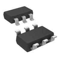
DAC121C081CIMKX/NOPB National Semiconductor, DAC121C081CIMKX/NOPB Datasheet - Page 4

DAC121C081CIMKX/NOPB
Manufacturer Part Number
DAC121C081CIMKX/NOPB
Description
DAC 12BIT MICROPWR I2C TSOT23-6
Manufacturer
National Semiconductor
Series
PowerWise®r
Datasheet
1.DAC121C081CISDNOPB.pdf
(24 pages)
Specifications of DAC121C081CIMKX/NOPB
Settling Time
6µs
Number Of Bits
12
Data Interface
I²C
Number Of Converters
1
Voltage Supply Source
Single Supply
Power Dissipation (max)
730µW
Operating Temperature
-40°C ~ 125°C
Mounting Type
Surface Mount
Package / Case
TSOT-23-6, TSOT-6
For Use With
DAC121C08XEB - BOARD EVAL FOR DAC121C081/5
Lead Free Status / RoHS Status
Lead free / RoHS Compliant
Other names
DAC121C081CIMKX
www.national.com
STATIC PERFORMANCE
ANALOG OUTPUT CHARACTERISTICS (V
Symbol
TC GE
Absolute Maximum Ratings
(Notes 1, 2)
If Military/Aerospace specified devices are required,
please contact the National Semiconductor Sales Office/
Distributors for availability and specifications.
Electrical Characteristics
Values shown in this table are design targets and are subject to change before product release.
The following specifications apply for V
limits apply for T
ZCED
ZCO
DNL
FSE
FSO
Supply Voltage, V
Voltage on any Input Pin
Input Current at Any Pin (Note 3)
Package Input Current (Note 3)
Power Consumption at T
ESD Susceptibility (Note 5)
Junction Temperature
Storage Temperature
INL
GE
ZE
I
OS
V
ADR0, ADR1 pins:
SDA, SCL pins:
A
Human Body Model
Machine Model
Charged Device Model (CDM)
Human Body Model
Machine Model
Charged Device Model (CDM)
, GND, V
Resolution
Monotonicity
Integral Non-Linearity
Differential Non-Linearity
Zero Code Error
Full-Scale Error
Gain Error
Zero Code Error Drift
Gain Error Tempco
Output Voltage Range(Note 10)
Zero Code Output
Full Scale Output
Output Short Circuit Current
(I
SOURCE
REF
MIN
, V
)
A
OUT
≤
Parameter
T
,
A
A
≤
= 25°C
T
MAX
and all other limits are at T
A
= +2.7V to +5.5V, V
−65°C to +150°C
OUT
−0.3V to +6.5V
−0.3V to +6.5V
)
See (Note 4)
I
I
All ones Loaded to DAC register
V
V
DAC121C085
DAC121C081
V
V
V
V
V
V
OUT
OUT
A
A
A
A
A
A
A
A
= 3V
= 5V
= 3V, I
= 5V, I
= 3V, I
= 5V, I
= 3V, V
= 5V, V
±10 mA
±20 mA
+150°C
= 0
= 0
2500V
1000V
5000V
1000V
250V
350V
OUT
OUT
OUT
OUT
OUT
OUT
REF
A
= 200 µA
= 200 µA
= 200 µA
= 200 µA
Conditions
= 0V, Input Code = FFFh.
= 0V, Input Code = FFFh.
= V
= 25°C, unless otherwise specified.
4
A
, C
Operating Ratings
Package Thermal Resistances
Soldering
Semiconductor's Reflow Temperature Profile specifications.
Refer to www.national.com/packaging. (Note 6)
Operating Temperature Range
Supply Voltage, V
Reference Voltage, V
Digital Input Voltage (Note 7)
Output Load
L
= 200 pF to GND, input code range 48 to 4047. Boldface
8-Lead MSOP
6-Lead TSOT
6-Lead LLP
Package
process
A
REFIN
(Note 9)
Typical
+0.18
−0.12
2.984
4.989
+2.2
−1.5
+1.1
−0.1
−0.2
−0.7
−1.0
must
−20
1.3
7.0
56
69
(Notes 1, 2)
comply
(Note 9)
Limits
−40°C
V
+0.6
−0.5
−0.7
−0.7
+10
V
12
12
+8
−8
REF
0
0
250°C/W
190°C/W
240°C/W
A
θ
≤
JA
with
+2.7V to 5.5V
T
0 to 1500 pF
0.0V to 5.5V
+1.0V to V
A
%FSR (max)
%FSR (max)
ppm FSR/°C
ppm FSR/°C
≤
LSB (max)
LSB (max)
LSB (min)
LSB (min)
mV (max)
Bits (min)
Bits (min)
(Limits)
V (max)
V (max)
V (min)
V (min)
+125°C
National
µV/°C
Units
mV
mV
mA
mA
V
V
A


