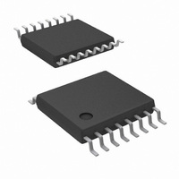
DAC128S085CIMTX/NOPB National Semiconductor, DAC128S085CIMTX/NOPB Datasheet - Page 20

DAC128S085CIMTX/NOPB
Manufacturer Part Number
DAC128S085CIMTX/NOPB
Description
IC DAC 12BIT 8CH RR OUT 16TSSOP
Manufacturer
National Semiconductor
Series
PowerWise®r
Datasheet
1.DAC128S085CISQNOPB.pdf
(24 pages)
Specifications of DAC128S085CIMTX/NOPB
Settling Time
6µs
Number Of Bits
12
Data Interface
Serial
Number Of Converters
8
Voltage Supply Source
Single Supply
Power Dissipation (max)
4.85mW
Operating Temperature
-40°C ~ 105°C
Mounting Type
Surface Mount
Package / Case
16-TSSOP
For Use With
DAC128S085EB - BOARD EVALUATION FOR DAC128S085
Lead Free Status / RoHS Status
Lead free / RoHS Compliant
Other names
DAC128S085CIMTX
Available stocks
Company
Part Number
Manufacturer
Quantity
Price
Company:
Part Number:
DAC128S085CIMTX/NOPB
Manufacturer:
ADI
Quantity:
9 384
www.national.com
2.5.3 Programmable Attenuator
Figure 16 shows one of the channels of the DAC128S085
being used as a single-quadrant multiplier. In this configura-
tion, an AC or DC signal can be driven into one of the refer-
ence pins. The SPI interface of the DAC can be used to
digitally attenuate the signal to any level from 0dB (full scale)
to 0V. This is accomplished without adding any noticeable
level of noise to the signal. An amplifier stage is shown in
Figure 16 as a reference for applications where the input sig-
nal requires amplification. Note how the AC signal in this
application is ac-coupled to the amplifier before being ampli-
fied. A separate bias voltage is used to set the common-mode
voltage for the DAC128S085's reference input to V
lowing the largest possible input swing. The multiplying band-
width of V
peak signal swing of 2V.
2.6 DSP/MICROPROCESSOR INTERFACING
Interfacing the DAC128S085 to microprocessors and DSPs
is quite simple. The following guidelines are offered to hasten
the design process.
2.6.1 ADSP-2101/ADSP2103 Interfacing
Figure 17 shows a serial interface between the DAC128S085
and the ADSP-2101/ADSP2103. The DSP should be set to
operate in the SPORT Transmit Alternate Framing Mode. It is
programmed through the SPORT control register and should
be configured for Internal Clock Operation, Active Low Fram-
ing and 16-bit Word Length. Transmission is started by writing
a word to the Tx register after the SPORT mode has been
enabled.
2.6.2 80C51/80L51 Interface
A serial interface between the DAC128S085 and the
80C51/80L51 microcontroller is shown in Figure 18. The
FIGURE 16. Programmable Attenuator
FIGURE 17. ADSP-2101/2103 Interface
REF1,2
is 360kHz with a V
CM
of 2.5V and a peak-to-
30016954
30016909
A
/ 2, al-
20
SYNC signal comes from a bit-programmable pin on the mi-
crocontroller. The example shown here uses port line P3.3.
This line is taken low when data is transmitted to the
DAC128S085. Since the 80C51/80L51 transmits 8-bit bytes,
only eight falling clock edges occur in the transmit cycle. To
load data into the DAC, the P3.3 line must be left low after the
first eight bits are transmitted. A second write cycle is initiated
to transmit the second byte of data, after which port line P3.3
is brought high. The 80C51/80L51 transmit routine must rec-
ognize that the 80C51/80L51 transmits data with the LSB first
while the DAC128S085 requires data with the MSB first.
2.6.3 68HC11 Interface
A serial interface between the DAC128S085 and the 68HC11
microcontroller is shown in Figure 19. The SYNC line of the
DAC128S085 is driven from a port line (PC7 in the figure),
similar to the 80C51/80L51.
The 68HC11 should be configured with its CPOL bit as a zero
and its CPHA bit as a one. This configuration causes data on
the MOSI output to be valid on the falling edge of SCLK. PC7
is taken low to transmit data to the DAC. The 68HC11 trans-
mits data in 8-bit bytes with eight falling clock edges. Data is
transmitted with the MSB first. PC7 must remain low after the
first eight bits are transferred. A second write cycle is initiated
to transmit the second byte of data to the DAC, after which
PC7 should be raised to end the write sequence.
2.6.4 Microwire Interface
Figure 20 shows an interface between a Microwire compatible
device and the DAC128S085. Data is clocked out on the rising
edges of the SK signal. As a result, the SK of the Microwire
device needs to be inverted before driving the SCLK of the
DAC128S085.
FIGURE 18. 80C51/80L51 Interface
FIGURE 20. Microwire Interface
FIGURE 19. 68HC11 Interface
30016910
30016911
30016912


