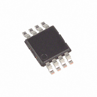
DS4432U+ Maxim Integrated Products, DS4432U+ Datasheet

DS4432U+
Specifications of DS4432U+
Related parts for DS4432U+
DS4432U+ Summary of contents
Page 1
... Settings Each for Sink and Source Modes ♦ I Applications 2 C-Compatible Serial Interface ♦ Low Cost ♦ Small Package (8-Pin µSOP) ♦ -40°C to +85°C Temperature Range ♦ 2.7V to 5.5V Operating Range PART DS4432U+ DS4432U+T& Denotes a lead(Pb)-free/RoHS-compliant package. T&R = Tape and reel. 7 OUT1 6 OUT0 5 ...
Page 2
Dual-Channel, I Current DAC ABSOLUTE MAXIMUM RATINGS Voltage Range SDA, and SCL CC Relative to Ground.............................................-0.5V to +6.0V Voltage Range on FS0, FS1, OUT0, OUT1 Relative to Ground..................................-0. Stresses beyond those listed under “Absolute Maximum ...
Page 3
Dual-Channel, I OUTPUT CURRENT SOURCE CHARACTERISTICS (continued +2.7V to +5.5V -40°C to +85°C.) CC PARAMETER SYMBOL Output Current Variation Due to Power-Supply Change Output Current Variation Due to Output-Voltage Change Output Leakage Current at Zero ...
Page 4
Dual-Channel, I Current DAC NAME PIN 2 SDA Serial Data. Input/output for I 2 SCL Serial Clock. Input for I FS1 3 Full-Scale Calibration Inputs. A resistor to ground on these pins determines the ...
Page 5
Dual-Channel, I (Applies to OUT0 and OUT1 2.7V to 5.0V, SDA = SCL = V CC otherwise noted.) INTEGRAL LINEARITY 1.0 RANGE FOR THE 50μA TO 200μA CURRENT 0.8 SOURCE AND SINK RANGE. 0.6 0.4 0.2 0 -0.2 ...
Page 6
Dual-Channel, I Current DAC Detailed Description 2 The DS4432 contains two I C adjustable current DACs that are each capable of sinking and sourcing current. Each output (OUT0 and OUT1) has 127 sink and 127 source settings that can be ...
Page 7
Dual-Channel, I Slave Devices: Slave devices send and receive data at the master’s request. Bus Idle or Not Busy: Time between STOP and START conditions when both SDA and SCL are inac- tive and in their logic-high states. When the ...
Page 8
Dual-Channel, I Current DAC 2 TYPICAL I C WRITE TRANSACTION MSB LSB START R/W READ/ SLAVE WRITE ADDRESS 2 EXAMPLE I C TRANSACTIONS 90h A) SINGLE BYTE WRITE SLAVE ...
Page 9
... Maxim cannot assume responsibility for use of any circuitry other than circuitry entirely embodied in a Maxim product. No circuit patent licenses are implied. Maxim reserves the right to change the circuitry and specifications without notice at any time. Maxim Integrated Products, 120 San Gabriel Drive, Sunnyvale, CA 94086 408-737-7600 _____________________ 9 © 2008 Maxim Integrated Products ...


