C8051F336-GMR Silicon Laboratories Inc, C8051F336-GMR Datasheet
C8051F336-GMR
Specifications of C8051F336-GMR
Available stocks


Related parts for C8051F336-GMR

C8051F336-GMR Summary of contents
Page 1
... HIGH-SPEED CONTROLLER CORE 16 kB 8051 CPU (25 MIPS) DEBUG CIRCUITRY Copyright © 2008 by Silicon Laboratories C8051F336/7/8/9 Supports crystal-less UART operation Low-power suspend mode with fast wake time Port 0 Port 1 P2.0– P2.3* P2.4* *P2.1–2.4 QFN24 Only OSCILLATOR 768 B SRAM POR WDT C8051F336/7/8 compati- ...
Page 2
... C8051F336/7/8/9 2 Rev. 1.0 ...
Page 3
... Window Detector In Single-Ended Mode .................................................. 46 7.3.2. Window Detector In Differential Mode....................................................... 47 7.4. ADC0 Analog Multiplexer (C8051F336/8 only).................................................. 48 8. Temperature Sensor (C8051F336/8 only) .............................................................. 51 9. 10-Bit Current Mode DAC (IDA0, C8051F336/8 only) ............................................ 52 9.1. IDA0 Output Scheduling .................................................................................... 52 9.1.1. Update Output On-Demand ...................................................................... 52 9.1.2. Update Output Based on Timer Overflow ................................................. 53 9 ...
Page 4
... C8051F336/7/8/9 14. Special Function Registers................................................................................... 78 15. Interrupts ................................................................................................................ 82 15.1. MCU Interrupt Sources and Vectors................................................................ 83 15.1.1. Interrupt Priorities.................................................................................... 83 15.1.2. Interrupt Latency ..................................................................................... 83 15.2. Interrupt Register Descriptions ........................................................................ 84 15.3. External Interrupts /INT0 and /INT1................................................................. 89 16. Flash Memory......................................................................................................... 91 16.1. Programming The Flash Memory .................................................................... 91 16.1.1. Flash Lock and Key Functions ................................................................ 91 16 ...
Page 5
... Enhanced Serial Peripheral Interface (SPI0) ..................................................... 167 23.1. Signal Descriptions........................................................................................ 168 23.1.1. Master Out, Slave In (MOSI)................................................................. 168 23.1.2. Master In, Slave Out (MISO)................................................................. 168 23.1.3. Serial Clock (SCK) ................................................................................ 168 23.1.4. Slave Select (NSS) ............................................................................... 168 23.2. SPI0 Master Mode Operation ........................................................................ 169 23.3. SPI0 Slave Mode Operation .......................................................................... 170 C8051F336/7/8/9 Rev.1.0 5 ...
Page 6
... C8051F336/7/8/9 23.4. SPI0 Interrupt Sources .................................................................................. 171 23.5. Serial Clock Phase and Polarity .................................................................... 171 23.6. SPI Special Function Registers ..................................................................... 173 24. Timers ................................................................................................................... 180 24.1. Timer 0 and Timer 1 ...................................................................................... 182 24.1.1. Mode 0: 13-bit Counter/Timer ............................................................... 182 24.1.2. Mode 1: 16-bit Counter/Timer ............................................................... 183 24.1.3. Mode 2: 8-bit Counter/Timer with Auto-Reload..................................... 184 24 ...
Page 7
... Figure 7.8. ADC0 Multiplexer Block Diagram .......................................................... 48 8. Temperature Sensor (C8051F336/8 only) Figure 8.1. Temperature Sensor Transfer Function ................................................ 51 9. 10-Bit Current Mode DAC (IDA0, C8051F336/8 only) Figure 9.1. IDA0 Functional Block Diagram ............................................................ 52 Figure 9.2. IDA0 Data Word Mapping ..................................................................... 53 10. Voltage Reference (C8051F336/8 only) Figure 10 ...
Page 8
... C8051F336/7/8/9 15. Interrupts 16. Flash Memory Figure 16.1. Security Byte Decoding ....................................................................... 93 17. Reset Sources Figure 17.1. Reset Sources ................................................................................... 100 Figure 17.2. Power-On and VDD Monitor Reset Timing ....................................... 101 18. Power Management Modes 19. Oscillators and Clock Selection Figure 19.1. Oscillator Options .............................................................................. 109 Figure 19.2. External 32.768 kHz Quartz Crystal Oscillator Connection Diagram 117 20 ...
Page 9
... Figure 25.8. PCA 8-Bit PWM Mode Diagram ........................................................ 210 Figure 25.9. PCA 9, 10 and 11-Bit PWM Mode Diagram ...................................... 211 Figure 25.10. PCA 16-Bit PWM Mode ................................................................... 212 Figure 25.11. PCA Module 2 with Watchdog Timer Enabled ................................ 213 26. C2 Interface Figure 26.1. Typical C2 Pin Sharing ...................................................................... 224 C8051F336/7/8/9 Rev.1.0 9 ...
Page 10
... List of Tables 1. System Overview 2. Ordering Information Table 2.1. Product Selection Guide ......................................................................... 18 3. Pin Definitions Table 3.1. Pin Definitions for the C8051F336/7/8/9 ................................................. 19 4. QFN-20 Package Specifications Table 4.1. QFN-20 Package Dimensions ................................................................ 23 Table 4.2. QFN-20 PCB Land Pattern Dimesions ................................................... 24 5. QFN-24 Package Specifications Table 5 ...
Page 11
... Table 23.1. SPI Slave Timing Parameters ............................................................ 179 24. Timers 25. Programmable Counter Array Table 25.1. PCA Timebase Input Options ............................................................. 203 Table 25.2. PCA0CPM and PCA0PWM Bit Settings for PCA Capture/Compare Mod- ules ..................................................................................................... 205 Table 25.3. Watchdog Timer Timeout Intervals1 ................................................... 214 26. C2 Interface C8051F336/7/8/9 Rev.1.0 11 ...
Page 12
... C8051F336/7/8/9 List of Registers SFR Definition 7.1. ADC0CF: ADC0 Configuration ...................................................... 41 SFR Definition 7.2. ADC0H: ADC0 Data Word MSB .................................................... 42 SFR Definition 7.3. ADC0L: ADC0 Data Word LSB ...................................................... 42 SFR Definition 7.4. ADC0CN: ADC0 Control ................................................................ 43 SFR Definition 7.5. ADC0GTH: ADC0 Greater-Than Data High Byte .......................... 44 SFR Definition 7.6. ADC0GTL: ADC0 Greater-Than Data Low Byte ............................ 44 SFR Definition 7 ...
Page 13
... SFR Definition 24.15. TMR3RLH: Timer 3 Reload Register High Byte ...................... 200 SFR Definition 24.16. TMR3L: Timer 3 Low Byte ....................................................... 200 SFR Definition 24.17. TMR3H Timer 3 High Byte ....................................................... 201 SFR Definition 25.1. PCA0CN: PCA Control .............................................................. 215 SFR Definition 25.2. PCA0MD: PCA Mode ................................................................ 216 C8051F336/7/8/9 Rev.1.0 13 ...
Page 14
... C8051F336/7/8/9 SFR Definition 25.3. PCA0PWM: PCA PWM Configuration ....................................... 217 SFR Definition 25.4. PCA0CPMn: PCA Capture/Compare Mode .............................. 218 SFR Definition 25.5. PCA0L: PCA Counter/Timer Low Byte ...................................... 219 SFR Definition 25.6. PCA0H: PCA Counter/Timer High Byte ..................................... 219 SFR Definition 25.7. PCA0CPLn: PCA Capture Module Low Byte ............................. 220 SFR Definition 25 ...
Page 15
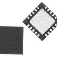
... Each device is specified for 2.7 to 3.6 V operation over the industrial temperature range (–40 to +85 °C). The Port I/O and RST pins are tolerant of input signals The C8051F336/7 are available in a 20- pin QFN package and the C8051F338/9 are available in a 24-pin QFN package. Both package options are lead-free and RoHS compliant ...
Page 16
... Byte XRAM Power Net VDD GND Precision 24.5 MHz Oscillator Low-Freq. Oscillator External XTAL1 Oscillator XTAL2 Circuit System Clock Configuration Figure 1.1. C8051F336/7 Block Diagram 16 Port I/O Configuration Digital Peripherals UART Timers Priority Crossbar PCA/ Decoder WDT SMBus SPI SYSCLK Crossbar Control ...
Page 17
... VDD SYSCLK GND Precision 24.5 MHz Oscillator Low-Freq. Oscillator External XTAL1 Oscillator XTAL2 Circuit System Clock Configuration Figure 1.2. C8051F338/9 Block Diagram C8051F336/7/8/9 Port I/O Configuration Digital Peripherals UART Port 0 Drivers Timers Priority Crossbar PCA/ Decoder WDT SMBus SPI Port 1 Drivers ...
Page 18
... C8051F336/7/8/9 2. Ordering Information Table 2.1. Product Selection Guide C8051F336- 768 Y C8051F337- 768 Y C8051F338- 768 Y C8051F339- 768 — — — — — — — — Y Rev.1 QFN-20 Y QFN- QFN-24 Y QFN-24 ...
Page 19
... Pin Definitions Table 3.1. Pin Definitions for the C8051F336/7/8/9 Name Pin Pin ’F336/7 ’F338 GND 2 3 RST C2CK C2D 5 6 P0. VREF P0 IDA0 P0. XTAL1 P0. XTAL2 P0 P0 P0. CNVSTR C8051F336/7/8/9 Type Description Power Supply Voltage. Ground. This ground connection is required. The center pad may optionally be connected to ground also ...
Page 20
... C8051F336/7/8/9 Table 3.1. Pin Definitions for the C8051F336/7/8/9 (Continued) Name Pin Pin ’F336/7 ’F338 P2.1 — 9 P2.2 — 8 P2.3 — 7 P2.4 — Type Description D I/O or Port 0. I/O or Port 1. I/O or Port 1. I/O or Port 1. I/O or Port 1. I/O or Port 1.4. ...
Page 21
... P0.0 1 GND 2 VDD 3 /RST/C2CK 4 P2.0/C2D 5 Figure 3.1. QFN-20 Pinout Diagram (Top View) C8051F336/7/8/9 C8051F336/7 Top View GND (optional) Rev.1.0 15 P0.6 14 P0.7 13 P1.0 12 P1.1 11 P1.2 21 ...
Page 22
... C8051F336/7/8/9 P0.1 1 P0.0 2 GND 3 VDD 4 /RST/C2CK 5 P2.4/C2D 6 Figure 3.2. QFN-24 Pinout Diagram (Top View) 22 C8051F338/9 Top View GND (optional) Rev.1.0 18 P1.0 17 P1.1 16 P1.2 15 P1.3 14 P1.4 13 P1.5 ...
Page 23
... This drawing conforms to the JEDEC Solid State Outline MO-220, variation VGGD except for custom features D2, E2 and L which are toleranced per supplier designation. 4. Recommended card reflow profile is per the JEDEC/IPC J-STD-020C specification for Small Body Components. C8051F336/7/8/9 Max Dimension Min 1. ...
Page 24
... C8051F336/7/8/9 Figure 4.2. QFN-20 Recommended PCB Land Pattern Table 4.2. QFN-20 PCB Land Pattern Dimesions Dimension Min C1 3.70 C2 3.70 E 0.50 X1 0.20 Notes: General 1. All dimensions shown are in millimeters (mm) unless otherwise noted. 2. Dimensioning and Tolerancing is per the ANSI Y14.5M-1994 specification. 3. This Land Pattern Design is based on the IPC-7351 guidelines. ...
Page 25
... Dimensioning and Tolerancing per ANSI Y14.5M-1994. 3. This drawing conforms to JEDEC Solid State Outline MO-220, variation WGGD except for custom features D2, E2 and L which are toleranced per supplier designation. 4. Recommended card reflow profile is per the JEDEC/IPC J-STD-020C specification for Small Body Components. C8051F336/7/8/9 Max Dimension Min 0. ...
Page 26
... C8051F336/7/8/9 Figure 5.2. QFN-24 Recommended PCB Land Pattern Table 5.2. QFN-24 PCB Land Pattern Dimesions Dimension Min C1 3.90 C2 3.90 E 0.50 BSC X1 0.20 Notes: General 1. All dimensions shown are in millimeters (mm) unless otherwise noted. 2. This Land Pattern Design is based on the IPC-7351 guidelines. Solder Mask Design 3. All metal pads are to be non-solder mask defined (NSMD). Clearance between the solder mask and the metal pad 60μ ...
Page 27
... Note: Stresses above those listed under “Absolute Maximum Ratings” may cause permanent damage to the device. This is a stress rating only and functional operation of the devices at those or any other conditions above those indicated in the operation listings of this specification is not implied. Exposure to maximum rating conditions for extended periods may affect device reliability. C8051F336/7/8/9 Conditions Min –55 – ...
Page 28
... C8051F336/7/8/9 6.2. Electrical Characteristics Table 6.2. Global Electrical Characteristics –40 to +85 °C, 25 MHz system clock unless otherwise specified. Parameter Conditions Digital Supply Voltage Normal Operation Writing or Erasing Flash Memory Digital Supply RAM Data Retention Voltage SYSCLK (System Clock) (Note 2) T (SYSCLK High Time) ...
Page 29
... Port I/O push-pull –10 mA, Port I/O push-pull OH Output Low Voltage µ Input High Voltage Input Low Voltage Input Leakage Weak Pullup Off Current Weak Pullup On, V C8051F336/7/8/9 Min Typ V – 0 – 0.1 DD — — — — 1.0 2.0 — — — ...
Page 30
... C8051F336/7/8/9 Table 6.4. Reset Electrical Characteristics –40 to +85 °C unless otherwise specified. Parameter Conditions RST Output Low Voltage RST Input Low Voltage RST Input Pullup Current RST = 0 POR Threshold ( RST Missing Clock Detector Time- Time from last system clock out rising edge to reset initiation ...
Page 31
... Using factory-calibrated settings Parameter Conditions Oscillator Frequency OSCLD = 11b Oscillator Supply Current 25 °C, V (from V ) OSCLCN Power Supply Sensitivity Constant Temperature Temperature Sensitivity Constant Supply C8051F336/7/8/9 Min Typ 24 24.5 = 3.0 V, — 450 DD — 0.12 — 60 Min Typ 3.0 V, — ...
Page 32
... C8051F336/7/8/9 Table 6.8. ADC0 Electrical Characteristics V = 3.0 V, VREF = 2.40 V (REFSL=0), DD Parameter DC Accuracy Resolution Integral Nonlinearity Differential Nonlinearity Offset Error Full Scale Error Offset Temperature Coefficient Dynamic performance (10 kHz sine-wave single-ended input below Full Scale, 200 ksps) Signal-to-Noise Plus Distortion Total Harmonic Distortion ...
Page 33
... Power Supply Rejection External Reference (REFBE = 0) Input Voltage Range Input Current Sample Rate = 200 ksps; VREF = 3.0 V Power Specifications Reference Bias Generator REFBE = ‘1’ or TEMPE = ‘1’ C8051F336/7/8/9 Min Typ — ± 0.2 — 2.25 — 23 — ...
Page 34
... C8051F336/7/8/9 Table 6.11. IDAC Electrical Characteristics – +85 °C, = 3.0 V Full-scale output current set unless otherwise specified. DD Parameter Conditions Static Performance Resolution Integral Nonlinearity Differential Nonlinearity Guaranteed Monotonic Output Compliance Range Offset Error Full Scale Error 2 mA Full Scale Output Current Full Scale Error Tempco ...
Page 35
... Input Bias Current Input Offset Voltage Power Supply Power Supply Rejection Power-up Time Supply Current at DC Mode 0 Mode 1 Mode 2 Mode 3 Note: Vcm is the common-mode voltage on CP0+ and CP0–. C8051F336/7/8/9 Min Typ — 100 — 200 — 250 — 350 — ...
Page 36
... C8051F336/7/8/9 6.3. Typical Performance Curves VDD = 3.6V 12.0 10.0 8.0 6.0 4.0 2.0 0 Figure 6.1. Normal Mode Digital Supply Current vs. Frequency VDD = 3.6V 6.0 5.0 4.0 3.0 2.0 1.0 0 Figure 6.2. Idle Mode Digital Supply Current vs. Frequency 36 VDD = 3.3V VDD = 3.0V VDD = 2 ...
Page 37
... ADC (ADC0, C8051F336/8 only) The ADC0 on the C8051F336 200 ksps, 10-bit successive-approximation-register (SAR) ADC with integrated track-and-hold and programmable window detector. The ADC is fully configurable under soft- ware control via Special Function Registers. The ADC0 operates in both Single-ended and Differential ...
Page 38
... C8051F336/7/8/9 7.1. Output Code Formatting The ADC is in Single-ended mode when the negative input is connected to GND. The ADC will be in Differ- ential mode when the negative input is connected to any other option. The output code format differs between Single-ended and Differential modes. The registers ADC0H and ADC0L contain the high and low bytes of the output conversion code from the ADC at the completion of each conversion ...
Page 39
... Timer 1, Timer 3 Overflow (AD0CM[2:0]=000, 001,010 011, 101) SAR Clocks AD0TM=1 SAR Clocks AD0TM=0 Figure 7.2. 10-Bit ADC Track and Conversion Example Timing C8051F336/7/8/9 for timer configuration. 40. A. ADC0 Timing for External Trigger Source Low Power Track Convert or Convert Track or Convert Convert B ...
Page 40
... C8051F336/7/8/9 7.2.3. Settling Time Requirements A minimum tracking time is required before each conversion to ensure that an accurate conversion is per- formed. This tracking time is determined by any series impedance, including the AMUX0 resistance, the the ADC0 sampling capacitance, and the accuracy required for the conversion. Note that in low-power tracking mode, three SAR clocks are used for tracking at the start of every conversion ...
Page 41
... Type 1 1 Reset SFR Address = 0xBC Bit Name 7:3 AD0SC[4:0] 2 AD0LJST 1:0 UNUSED C8051F336/7/8 AD0LJST R Function ADC0 SAR Conversion Clock Period Bits. SAR Conversion clock is derived from system clock by the fol- lowing equation, where AD0SC refers to the 5-bit value held in bits AD0SC4–0. SAR Conversion clock requirements are given in the ADC specification table ...
Page 42
... C8051F336/7/8/9 SFR Definition 7.2. ADC0H: ADC0 Data Word MSB Bit 7 6 Name Type 0 0 Reset SFR Address = 0xBE Bit Name 7:0 ADC0H[7:0] ADC0 Data Word High-Order Bits. For AD0LJST = 0: Bits 7–2 are the sign extension of Bit1. Bits 1–0 are the upper 2 bits of the 10-bit ADC0 Data Word. For AD0LJST = 1: Bits 7– ...
Page 43
... ADC0 start-of-conversion source is write of ‘1’ to AD0BUSY. 001: ADC0 start-of-conversion source is overflow of Timer 0. 010: ADC0 start-of-conversion source is overflow of Timer 2. 011: ADC0 start-of-conversion source is overflow of Timer 1. 100: ADC0 start-of-conversion source is rising edge of external CNVSTR. 101: ADC0 start-of-conversion source is overflow of Timer 3. 11x: Reserved. C8051F336/7/8 AD0BUSY AD0WINT R/W R/W ...
Page 44
... C8051F336/7/8/9 7.3. Programmable Window Detector The ADC Programmable Window Detector continuously compares the ADC0 output registers to user-pro- grammed limits, and notifies the system when a desired condition is detected. This is especially effective in an interrupt-driven system, saving code space and CPU bandwidth while delivering faster system response times ...
Page 45
... ADC0LTH[7:0] ADC0 Less-Than Data Word High-Order Bits. SFR Definition 7.8. ADC0LTL: ADC0 Less-Than Data Low Byte Bit 7 6 Name Type 0 0 Reset SFR Address = 0xC5 Bit Name 7:0 ADC0LTL[7:0] ADC0 Less-Than Data Word Low-Order Bits. C8051F336/7/8 ADC0LTH[7:0] R Function ADC0LTL[7:0] R/W 0 ...
Page 46
... C8051F336/7/8/9 7.3.1. Window Detector In Single-Ended Mode Figure 7.4 shows two example window comparisons for right-justified, single-ended data, with ADC0LTH:ADC0LTL = 0x0080 (128d) and ADC0GTH:ADC0GTL = 0x0040 (64d). In single-ended mode, the input voltage can range from ‘0’ to VREF x (1023/1024) with respect to GND, and is represented by a 10-bit unsigned integer value ...
Page 47
... ADC0LTH:ADC0LTL 0x0FC0 0x0000 VREF x (-1/512) 0xFFC0 ADC0GTH:ADC0GTL 0xFF80 AD0WINT not affected 0x8000 -VREF Figure 7.7. ADC Window Compare Example: Left-Justified Differential Data C8051F336/7/8/9 ADC0LT registers (if ADC0H:ADC0L < 0xFFFF ADC0H:ADC0L Input Voltage (Px.x - Px.x) VREF x (511/512) 0x01FF 0x0041 VREF x (64/512) 0x0040 0x003F ...
Page 48
... C8051F336/7/8/9 7.4. ADC0 Analog Multiplexer (C8051F336/8 only) ADC0 on the C8051F336/8 has two analog multiplexers, referred to collectively as AMUX0. AMUX0 selects the positive and negative inputs to the ADC. Any of the following may be selected as the positive input: Port I/O pins, the on-chip temperature sensor, or the positive power supply (V following may be selected as the negative input: Port I/O pins, V the negative input, ADC0 operates in Single-ended Mode ...
Page 49
... C8051F336/7/8 AMX0P[4: Function P0.0 P0.1 P0.2 P0.3 P0.4 P0.5 P0.6 P0.7 P1.0 P1.1 P1.2 P1.3 P1 ...
Page 50
... C8051F336/7/8/9 SFR Definition 7.10. AMX0N: AMUX0 Negative Channel Select Bit 7 6 Name R R Type 0 0 Reset SFR Address = 0xBA Bit Name 7:5 UNUSED Unused. Read = 000b; Write = Don’t Care. 4:0 AMX0N[4:0] AMUX0 Negative Input Selection. 00000: 00001: 00010: 00011: 00100: ...
Page 51
... Temperature Sensor (C8051F336/8 only) An on-chip temperature sensor is included on the C8051F336/8 which can be directly accessed via the ADC multiplexer in single-ended configuration. To use the ADC to measure the temperature sensor, the positive ADC mux channel should be configured to connect to the temperature sensor and the negative ADC mux channel should be configured to connect to GND ...
Page 52
... C8051F336/7/8/9 9. 10-Bit Current Mode DAC (IDA0, C8051F336/8 only) The C8051F336/8 device includes a 10-bit current-mode Digital-to-Analog Converter (IDAC). The maxi- mum current output of the IDAC can be adjusted for three different current settings; 0.5 mA, 1 mA, and 2 mA. The IDAC is enabled or disabled with the IDA0EN bit in the IDA0 Control Register (see SFR Defini- tion 9 ...
Page 53
... Figure 9.2. IDA0 Data Word Mapping The full-scale output current of the IDAC is selected using the IDA0OMD bits (IDA0CN[1:0]). By default, the IDAC is set to a full-scale output current of 2 mA. The IDA0OMD bits can also be configured to provide full-scale output currents 0.5 mA, as shown in SFR Definition 9.1. C8051F336/7/8 ...
Page 54
... C8051F336/7/8/9 SFR Definition 9.1. IDA0CN: IDA0 Control Bit 7 6 IDA0EN IDA0CM[2:0] Name R/W Type 0 1 Reset SFR Address = 0xB9 Bit Name 7 IDA0EN IDA0 Enable. 0: IDA0 Disabled. 1: IDA0 Enabled. 6:4 IDA0CM[2:0] IDA0 Update Source Select bits. 000: DAC output updates on Timer 0 overflow. ...
Page 55
... Bit 7 6 IDA0[1:0] Name R/W Type 0 0 Reset SFR Address = 0x96 Bit Name 7:6 IDA0[1:0] IDA0 Data Word Low-Order Bits. Lower 2 bits of the 10-bit IDA0 Data Word. 5:0 Unused Unused. Read = 000000b. Write = Don’t care. C8051F336/7/8 IDA0[9:2] R Function Function Rev.1.0 ...
Page 56
... C8051F336/7/8/9 10. Voltage Reference (C8051F336/8 only) The Voltage reference multiplexer for the ADC is configurable to use an externally connected voltage refer- ence, the on-chip reference voltage generator routed to the VREF pin, or the V (see Figure 10.1). The REFSL bit in the Reference Control register (REF0CN, SFR Definition 10.1) selects the reference source for the ADC. For an external source or the on-chip reference, REFSL should be set to ‘ ...
Page 57
... Internal Temperature Sensor on. 1 BIASE Internal Analog Bias Generator Enable Bit. 0: Internal Bias Generator off. 1: Internal Bias Generator on. 0 REFBE On-chip Reference Buffer Enable Bit. 0: On-chip Reference Buffer off. 1: On-chip Reference Buffer on. Internal voltage reference driven on the V C8051F336/7/8 REFSL TEMPE R R R/W R/W 0 ...
Page 58
... C8051F336/7/8/9 11. Comparator0 C8051F336/7/8/9 devices include an on-chip programmable voltage comparator, Comparator0, shown in Figure 11.1. The Comparator offers programmable response time and hysteresis, an analog input multiplexer, and two outputs that are optionally available at the Port pins: a synchronous “latched” output (CP0 asyn- chronous “raw” output (CP0A). The asynchronous CP0A signal is available even when the system clock is not active ...
Page 59
... Comparator rising-edge occurrence. Once set, these bits remain set until cleared by soft- ware. The Comparator rising-edge interrupt mask is enabled by setting CP0RIE to a logic 1. The Comparator0 falling-edge interrupt mask is enabled by setting CP0FIE to a logic 1. C8051F336/7/8 0.25 V without damage or upset. The complete Comparator elec- OUT ...
Page 60
... C8051F336/7/8/9 The output state of the Comparator can be obtained at any time by reading the CP0OUT bit. The Compar- ator is enabled by setting the CP0EN bit to logic 1, and is disabled by clearing this bit to logic 0. Note that false rising edges and falling edges can be detected when the comparator is first powered changes are made to the hysteresis or response time control bits ...
Page 61
... CP0HYP[1:0] Comparator0 Positive Hysteresis Control Bits. 00: Positive Hysteresis Disabled. 01: Positive Hysteresis = 5 mV. 10: Positive Hysteresis = 10 mV. 11: Positive Hysteresis = 20 mV. 1:0 CP0HYN[1:0] Comparator0 Negative Hysteresis Control Bits. 00: Negative Hysteresis Disabled. 01: Negative Hysteresis = 5 mV. 10: Negative Hysteresis = 10 mV. 11: Negative Hysteresis = 20 mV. C8051F336/7/8 CP0FIF CP0HYP[1:0] R/W R/W R/W 0 ...
Page 62
... C8051F336/7/8/9 SFR Definition 11.2. CPT0MD: Comparator0 Mode Selection Bit 7 6 CP0RIE Name R R Type 0 0 Reset SFR Address = 0x9D Bit Name 7:6 Unused Unused. Read = 00b, Write = Don’t Care. 5 CP0RIE Comparator0 Rising-Edge Interrupt Enable. 0: Comparator0 Rising-edge interrupt disabled. 1: Comparator0 Rising-edge interrupt enabled. ...
Page 63
... Comparator Multiplexer C8051F336/7/8/9 devices include an analog input multiplexer to connect Port I/O pins to the comparator inputs. The Comparator0 inputs are selected in the CPT0MX register (SFR Definition 11.3). The CMX0P1–CMX0P0 bits select the Comparator0 positive input; the CMX0N1–CMX0N0 bits select the Comparator0 negative input ...
Page 64
... C8051F336/7/8/9 SFR Definition 11.3. CPT0MX: Comparator0 MUX Selection Bit 7 6 CMX0N[3:0] Name R/W Type 1 1 Reset SFR Address = 0x9F Bit Name 7:4 CMX0N[3:0] Comparator0 Negative Input MUX Selection. 0000: 0001: 0010: 0011: 0100: 0101: 0110: 0111: 1000: 1001: 1010-1111: 3:0 CMX0P[3:0] Comparator0 Positive Input MUX Selection. ...
Page 65
... ACCUMULATOR RESET CLOCK STOP IDLE Figure 12.1. CIP-51 Block Diagram C8051F336/7/8/9 Reset Input Power Management Modes On-chip Debug Logic Program and Data Memory Security DATA BUS B REGISTER STACK POINTER ...
Page 66
... C8051F336/7/8/9 With the CIP-51's maximum system clock at 25 MHz, it has a peak throughput of 25 MIPS. The CIP-51 has a total of 109 instructions. The table below shows the total number of instructions that require each execu- tion time. Clocks to Execute 1 Number of Instructions 26 12.1. Instruction Set The instruction set of the CIP-51 System Controller is fully compatible with the standard MCS-51™ ...
Page 67
... ORL direct direct byte ORL direct, #data OR immediate to direct byte XRL A, Rn Exclusive-OR Register to A XRL A, direct Exclusive-OR direct byte to A XRL A, @Ri Exclusive-OR indirect RAM to A XRL A, #data Exclusive-OR immediate to A XRL direct, A Exclusive- direct byte C8051F336/7/8/9 Bytes Rev.1.0 Clock Cycles ...
Page 68
... C8051F336/7/8/9 Table 12.1. CIP-51 Instruction Set Summary (Continued) Mnemonic Description XRL direct, #data Exclusive-OR immediate to direct byte CLR A Clear A CPL A Complement Rotate A left RLC A Rotate A left through Carry RR A Rotate A right RRC A Rotate A right through Carry SWAP A Swap nibbles of A Data Transfer ...
Page 69
... Compare immediate to Register and jump if not equal CJNE @Ri, #data, rel Compare immediate to indirect and jump if not equal DJNZ Rn, rel Decrement Register and jump if not zero DJNZ direct, rel Decrement direct byte and jump if not zero NOP No operation C8051F336/7/8/9 Bytes Rev.1.0 Clock Cycles ...
Page 70
... C8051F336/7/8/9 Notes on Registers, Operands and Addressing Modes Register R0–R7 of the currently selected register bank. @Ri - Data RAM location addressed indirectly through R0 or R1. rel - 8-bit, signed (twos complement) offset relative to the first byte of the following instruction. Used by SJMP and all conditional jumps. direct - 8-bit internal data location’s address. This could be a direct-access Data RAM location (0x00– ...
Page 71
... The DPL register is the low byte of the 16-bit DPTR. SFR Definition 12.2. DPH: Data Pointer High Byte Bit 7 6 Name Type 0 0 Reset SFR Address = 0x83 Bit Name 7:0 DPH[7:0] Data Pointer High. The DPH register is the high byte of the 16-bit DPTR. C8051F336/7/8 DPL[7:0] R Function DPH[7:0] R ...
Page 72
... C8051F336/7/8/9 SFR Definition 12.3. SP: Stack Pointer Bit 7 6 Name Type 0 0 Reset SFR Address = 0x81 Bit Name 7:0 SP[7:0] Stack Pointer. The Stack Pointer holds the location of the top of the stack. The stack pointer is incre- mented before every PUSH operation. The SP register defaults to 0x07 after reset. ...
Page 73
... The OV bit is cleared the ADD, ADDC, SUBB, MUL, and DIV instructions in all other cases User Flag 1. This is a bit-addressable, general purpose flag for use under software control. 0 PARITY Parity Flag. This bit is set to logic 1 if the sum of the eight bits in the accumulator is odd and cleared if the sum is even. C8051F336/7/8 RS[1:0] R/W R Function Rev ...
Page 74
... The memory organization of the CIP-51 System Controller is similar to that of a standard 8051. There are two separate memory spaces: program memory and data memory. Program and data memory share the same address space but are accessed via different instruction types. The memory organization of the C8051F336/7/8/9 device family is shown in Figure 13.1 PROGRAM/DATA MEMORY (FLASH) ...
Page 75
... Program Memory The CIP-51 core has program memory space. The C8051F336/7/8/9 implements this pro- gram memory space as in-system, re-programmable Flash memory, organized in a contiguous block from addresses 0x0000 to 0x3DFF. The address 0x3DFF serves as the security lock byte for the device, and addresses above 0x3DFF are reserved ...
Page 76
... SFR space. Instructions using indirect addressing above 0x7F access the upper 128 bytes of data memory. Figure 13.1 illustrates the data memory organization of the C8051F336/7/8/9. 13.2.1.1. General Purpose Registers The lower 32 bytes of data memory, locations 0x00 through 0x1F, may be addressed as four banks of gen- eral-purpose registers ...
Page 77
... MOVX command, effectively selecting a 256-byte page of RAM. Since the upper (unused) bits of the register are always zero, the PGSEL determines which page of XRAM is accessed. For Example: If EMI0CN = 0x01, addresses 0x0100 through 0x01FF will be accessed. C8051F336/7/8 R/W R/W ...
Page 78
... SFRs used to configure and access the sub-systems unique to the C8051F336/7/8/9. This allows the addition of new functionality while retaining compatibility with the MCS- 51™ instruction set. Table 14.1 lists the SFRs implemented in the C8051F336/7/8/9 device family. The SFR registers are accessed anytime the direct addressing mode is used to access memory locations from 0x80 to 0xFF ...
Page 79
... Current Mode DAC0 High IDA0H 0x96 Current Mode DAC0 Low IDA0L 0xA8 Interrupt Enable IE 0xB8 Interrupt Priority IP 0xE4 INT0/INT1 Configuration IT01CF 0xB3 Internal Oscillator Calibration OSCICL 0xB2 Internal Oscillator Control OSCICN 0xE3 Low-Frequency Oscillator Control OSCLCN C8051F336/7/8/9 Rev.1.0 Page 181 110 ...
Page 80
... C8051F336/7/8/9 Table 14.2. Special Function Registers (Continued) SFRs are listed in alphabetical order. All undefined SFR locations are reserved Register Address Description 0xB1 External Oscillator Control OSCXCN 0x80 Port 0 Latch P0 0xFE Port 0 Mask Configuration P0MASK 0xFD Port 0 Match Configuration P0MAT 0xF1 Port 0 Input Mode Configuration ...
Page 81
... Timer/Counter 3 Reload High TMR3RLH 0x92 Timer/Counter 3 Reload Low TMR3RLL 0xFF V Monitor Control VDM0CN DD 0xE1 Port I/O Crossbar Control 0 XBR0 0xE2 Port I/O Crossbar Control 1 XBR1 C8051F336/7/8/9 Rev.1.0 Page 57 105 165 164 149 148 144 146 150 72 174 176 175 176 ...
Page 82
... C8051F336/7/8/9 15. Interrupts The C8051F336/7/8/9 includes an extended interrupt system supporting a total of 14 interrupt sources with two priority levels. The allocation of interrupt sources between on-chip peripherals and external input pins varies according to the specific version of the device. Each interrupt source has one or more associated interrupt-pending flag(s) located in an SFR ...
Page 83
... MCU Interrupt Sources and Vectors The C8051F336/7/8/9 MCUs support 14 interrupt sources. Software can simulate an interrupt by setting any interrupt-pending flag to logic 1. If interrupts are enabled for the flag, an interrupt request will be gener- ated and the CPU will vector to the ISR address associated with the interrupt-pending flag. MCU interrupt sources, associated vector addresses, priority order and control bits are summarized in Table 15 ...
Page 84
... C8051F336/7/8/9 Table 15.1. Interrupt Summary Interrupt Source Interrupt Vector Reset 0x0000 External Interrupt 0 0x0003 (/INT0) Timer 0 Overflow 0x000B External Interrupt 1 0x0013 (/INT1) Timer 1 Overflow 0x001B UART0 0x0023 Timer 2 Overflow 0x002B SPI0 0x0033 SMB0 0x003B Port Match 0x0043 ADC0 Window Com- 0x004B ...
Page 85
... This bit sets the masking of the Timer 0 interrupt. 0: Disable all Timer 0 interrupt. 1: Enable interrupt requests generated by the TF0 flag. 0 EX0 Enable External Interrupt 0. This bit sets the masking of External Interrupt 0. 0: Disable external interrupt 0. 1: Enable interrupt requests generated by the /INT0 input. C8051F336/7/8 ET2 ES0 ET1 R/W R/W ...
Page 86
... C8051F336/7/8/9 SFR Definition 15.2. IP: Interrupt Priority Bit 7 6 PSPI0 Name R R/W Type 1 0 Reset SFR Address = 0xB8; Bit-Addressable Bit Name 7 UNUSED Unused. Read = 1, Write = Don't Care. 6 PSPI0 Serial Peripheral Interface (SPI0) Interrupt Priority Control. This bit sets the priority of the SPI0 interrupt. ...
Page 87
... This bit sets the masking of the Port Match Event interrupt. 0: Disable all Port Match interrupts. 1: Enable interrupt requests generated by a Port Match. 0 ESMB0 Enable SMBus (SMB0) Interrupt. This bit sets the masking of the SMB0 interrupt. 0: Disable all SMB0 interrupts. 1: Enable interrupt requests generated by SMB0. C8051F336/7/8 ECP0 EPCA0 EADC0 EWADC0 R/W ...
Page 88
... C8051F336/7/8/9 SFR Definition 15.4. EIP1: Extended Interrupt Priority 1 Bit 7 6 PT3 Reserved Name R/W R/W Type 0 0 Reset SFR Address = 0xF6 Bit Name 7 PT3 Timer 3 Interrupt Priority Control. This bit sets the priority of the Timer 3 interrupt. 0: Timer 3 interrupts set to low priority level. ...
Page 89
... The external interrupt source must hold the input active until the interrupt request is recognized. It must then deactivate the interrupt request before execution of the ISR completes or another interrupt request will be generated. C8051F336/7/8/9 (Section “24.1. Timer 0 and Timer 1” on page IT1 IN1PL ...
Page 90
... C8051F336/7/8/9 SFR Definition 15.5. IT01CF: INT0/INT1 Configuration Bit 7 6 IN1PL IN1SL[2:0] Name R/W Type 0 0 Reset SFR Address = 0xE4 Bit Name 7 IN1PL /INT1 Polarity. 0: /INT1 input is active low. 1: /INT1 input is active high. 6:4 IN1SL[2:0] /INT1 Port Pin Selection Bits. These bits select which Port pin is assigned to /INT1. Note that this pin assignment is independent of the Crossbar ...
Page 91
... Write the first key code to FLKEY: 0xA5. 5. Write the second key code to FLKEY: 0xF1. 6. Using the MOVX instruction, write a data byte to any location within the 512-byte page to be erased. 7. Clear the PSWE and PSEE bits. C8051F336/7/8/9 for complete Flash memory electrical Section “26. C2 Interface” Rev.1.0 ...
Page 92
... C8051F336/7/8/9 16.1.3. Flash Write Procedure Flash bytes are programmed by software with the following sequence: 1. Disable interrupts (recommended). 2. Erase the 512-byte Flash page containing the target location, as described in 3. Set the PSWE bit (register PSCTL). 4. Clear the PSEE bit (register PSCTL). 5. Write the first key code to FLKEY: 0xA5. ...
Page 93
... Flash pages are locked (any bit of the Lock Byte is ‘0’). An example is shown in Figure 16.1. Security Lock Byte: 1s Complement: Flash pages locked: Figure 16.1. Security Byte Decoding C8051F336/7/8/9 11111101b 00000010b 3 (First two Flash pages + Lock Byte Page) Rev.1.0 Section “13. Memory ...
Page 94
... The level of Flash security depends on the Flash access method. The three Flash access methods that can be restricted are reads, writes, and erases from the C2 debug interface, user firmware executing on unlocked pages, and user firmware executing on locked pages. Table 16.1 summarizes the Flash security features of the C8051F336/7/8/9 devices. Table 16.1. Flash Security Summary Action ...
Page 95
... Flash operation has been completed and interrupts have been re-enabled by software. 10.Make certain that the Flash write and erase pointer variables are not located in XRAM. See your compiler documentation for instructions regarding how to explicitly locate variables in different memory C8051F336/7/8/9 monitor DD rise time specification met ...
Page 96
... C8051F336/7/8/9 areas. 11. Add address bounds checking to the routines that write or erase Flash memory to ensure that a routine called with an illegal address does not result in modification of the Flash. 16.4.3. System Clock 12.If operating from an external crystal, be advised that crystal performance is susceptible to electrical interference and is sensitive to layout and to changes in temperature. If the system is operating in an electrically noisy environment, use the internal oscillator or use an external CMOS clock ...
Page 97
... Setting this bit allows writing a byte of data to the Flash program memory using the MOVX write instruction. The Flash location should be erased before writing data. 0: Writes to Flash program memory disabled. 1: Writes to Flash program memory enabled; the MOVX write instruction targets Flash memory. C8051F336/7/8 ...
Page 98
... C8051F336/7/8/9 SFR Definition 16.2. FLKEY: Flash Lock and Key Bit 7 6 Name Type 0 0 Reset SFR Address = 0xB7 Bit Name 7:0 FLKEY[7:0] Flash Lock and Key Register. Write: This register provides a lock and key function for Flash erasures and writes. Flash writes and erases are enabled by writing 0xA5 followed by 0xF1 to the FLKEY regis- ter ...
Page 99
... This bit enables the Flash read one-shot (recommended). If the Flash one-shot is dis- abled, the Flash sense amps are enabled for a full clock cycle during Flash reads, increasing the device power consumption. 0: Flash one-shot disabled. 1: Flash one-shot enabled. 6:0 Reserved Reserved. Must Write 0000000b. C8051F336/7/8 Reserved Reserved Reserved R/W ...
Page 100
... C8051F336/7/8/9 17. Reset Sources Reset circuitry allows the controller to be easily placed in a predefined default condition. Upon entering this reset state, the following events occur: CIP-51 halts program execution Special Function Registers (SFRs) are initialized to their defined reset values External Port pins are forced to a known state Interrupts and timers are disabled ...
Page 101
... The V power-on reset. 2.70 V RST 2.55 2.0 1.0 /RST Logic HIGH Logic LOW Figure 17.2. Power-On and V C8051F336/7/8/9 ramps from ramp time is 1 ms; slower ramp times may DD reaches the V level. For ramp times less than DD RST ) is typically less than 0.3 ms ...
Page 102
... C8051F336/7/8/9 17.2. Power-Fail Reset / V DD When a power-down transition or power irregularity causes V monitor will drive the RST pin low and hold the CIP- reset state (see Figure 17.2). When level above V , the CIP-51 will be released from the reset state. Note that even though internal data ...
Page 103
... MCD reset, the MCDRSF flag (RSTSRC.2) will read ‘1’, signifying the MCD as the reset source; otherwise, this bit reads ‘0’. Writing a ‘1’ to the MCDRSF bit enables the Missing Clock Detector; writing a ‘0’ disables it. The state of the RST pin is unaffected by this reset. C8051F336/7/8/9 Monitor Control DD ...
Page 104
... C8051F336/7/8/9 17.5. Comparator0 Reset Comparator0 can be configured as a reset source by writing a ‘1’ to the C0RSEF flag (RSTSRC.5). Comparator0 should be enabled and allowed to settle prior to writing to C0RSEF to prevent any turn-on chatter on the output from generating an unwanted reset. The Comparator0 reset is active-low: if the non- inverting input voltage (on CP0+) is less than the inverting input voltage (on CP0-), the device is put into the reset state. After a Comparator0 reset, the C0RSEF flag (RSTSRC.5) will read ‘ ...
Page 105
... WDTRSF Watchdog Timer Reset Flag. N/A 2 MCDRSF Missing Clock Detector Enable and Flag. 1 PORSF Power- Reset Flag, and V Reset Enable. 0 PINRSF HW Pin Reset Flag. Note: Do not use read-modify-write operations on this register C8051F336/7/8 SWRSF WDTRSF MCDRSF R/W R/W R Varies Varies Write Don’t care. ...
Page 106
... Suspend mode is controlled by the SUSPEND bit in the OSCICN register (SFR Definition 19.3). Although the C8051F336/7/8/9 has Idle, Stop, and Suspend modes available, more control over the device power can be achieved by enabling/disabling individual peripherals as needed. Each analog peripheral can be disabled when not in use and placed in low power mode. Digital peripherals, such as timers or serial buses, draw little power when they are not in use ...
Page 107
... If Suspend mode is ter- minated by an internal or external reset, the CIP-51 performs a normal reset sequence and begins program execution at address 0x0000. C8051F336/7/8/9 Section “17.6. PCA Watchdog Section “24.3. Timer 3” on page Rev.1.0 Section “ ...
Page 108
... C8051F336/7/8/9 SFR Definition 18.1. PCON: Power Control Bit 7 6 Name Type 0 0 Reset SFR Address = 0x87 Bit Name 7:2 GF[5:0] General Purpose Flags 5–0. These are general purpose flags for use under software control. 1 STOP Stop Mode Select. Setting this bit will place the CIP-51 in Stop mode. This bit will always be read as 0. ...
Page 109
... Oscillators and Clock Selection C8051F336/7/8/9 devices include a programmable internal high-frequency oscillator, a programmable internal low-frequency oscillator, and an external oscillator drive circuit. The internal high-frequency oscilla- tor can be enabled/disabled and calibrated using the OSCICN and OSCICL registers, as shown in Figure 19.1. The internal low-frequency oscillator can be enabled/disabled and calibrated using the OSCLCN register ...
Page 110
... C8051F336/7/8/9 SFR Definition 19.1. CLKSEL: Clock Select Bit 7 6 Name R R Type 0 0 Reset SFR Address = 0xA9 Bit Name 7:2 UNUSED Unused. Read = 000000b; Write = Don’t Care 1:0 CLKSL[1:0] System Clock Source Select Bits. 00: SYSCLK derived from the Internal High-Frequency Oscillator and scaled per the IFCN bits in register OSCICN ...
Page 111
... The internal oscillator period caPara1n be adjusted via the OSCICL register as defined by SFR Definition 19.2. On C8051F336/7/8/9 devices, OSCICL is factory calibrated to obtain a 24.5 MHz base frequency. The system clock may be derived from the programmed internal oscillator divided defined by the IFCN bits in register OSCICN ...
Page 112
... C8051F336/7/8/9 SFR Definition 19.3. OSCICN: Internal H-F Oscillator Control Bit 7 6 IOSCEN IFRDY SUSPEND Name R/W R Type 1 1 Reset SFR Address = 0xB2 Bit Name 7 IOSCEN Internal H-F Oscillator Enable Bit. 0: Internal H-F Oscillator Disabled. 1: Internal H-F Oscillator Enabled. 6 IFRDY Internal H-F Oscillator Frequency Ready Flag. ...
Page 113
... Programmable Internal Low-Frequency (L-F) Oscillator All C8051F336/7/8/9 devices include a programmable low-frequency internal oscillator, which is calibrated to a nominal frequency of 80 kHz. The low-frequency oscillator circuit includes a divider that can be changed to divide the clock using the OSCLD bits in the OSCLCN register (see SFR Defi- nition 19.4). Additionally, the OSCLF[3:0] bits can be used to adjust the oscillator’ ...
Page 114
... C8051F336/7/8/9 19.4. External Oscillator Drive Circuit The external oscillator circuit may drive an external crystal, ceramic resonator, capacitor network. A CMOS clock may also provide a clock input. For a crystal or ceramic resonator configuration, the crys- tal/resonator must be wired across the XTAL1 and XTAL2 pins as shown in Option 1 of Figure 19. MΩ ...
Page 115
... MHz 100 1.5 MHz < f ≤ 4 MHz 101 4 MHz < f ≤ 10 MHz 110 10 MHz < f ≤ 30 MHz 111 C8051F336/7/8 R Function Crystal Mode RC Mode f ≤ ...
Page 116
... C8051F336/7/8/9 19.4.1. External Crystal Example If a crystal or ceramic resonator is used as an external oscillator source for the MCU, the circuit should be configured as shown in Figure 19.1, Option 1. The External Oscillator Frequency Control value (XFCN) should be chosen from the Crystal column of the table in SFR Definition 19.5 (OSCXCN register). For example ...
Page 117
... Equation 19.1. RC Mode Oscillator Frequency For example: If the frequency desired is 100 kHz, let R = 246 kΩ and pF 1.23 1. 246 0.1 MHz = 100 kHz Referring to the table in SFR Definition 19.5, the required XFCN setting is 010b. C8051F336/7/8/9 XTAL1 10MΩ XTAL2 32.768 kHz 22pF* 3 × ...
Page 118
... C8051F336/7/8/9 19.4.3. External Capacitor Example If a capacitor is used as an external oscillator for the MCU, the circuit should be configured as shown in Figure 19.1, Option 3. The capacitor should be no greater than 100 pF; however for very small capacitors, the total capacitance may be dominated by parasitic capacitance in the PCB layout. To determine the required External Oscillator Frequency Control value (XFCN) in the OSCXCN Register, select the capaci- tor to be used and find the frequency of oscillation according to Equation 19 ...
Page 119
... Figure 20.4. Port pin P2.4 on the C8051F338/9 and P2.0 on the C8051F336/7 can be used as GPIO and are shared with the C2 Interface Data signal (C2D). The designer has complete control over which functions are assigned, limited only by the number of physical I/O pins ...
Page 120
... C8051F336/7/8/9 20.1. Port I/O Modes of Operation Port pins P0.0 - P2.3 use the Port I/O cell shown in Figure 20.2. Each Port I/O cell can be configured by software for analog I/O or digital I/O using the PnMDIN registers. On reset, all Port I/O cells default to a high impedance state with weak pull-ups enabled. Until the crossbar is enabled (XBARE = ‘1’), both the high and low port I/O drive circuits are explicitly disabled on all crossbar pins ...
Page 121
... Figure 20.3 shows the input current characteristics of port pins driven above VDD. The port pin requires 150 µA peak overdrive current when its voltage reaches approximately (VDD + 0.7 V Vtest I/O Cell + Port I/O Overdrive Test Circuit Figure 20.3. Port I/O Overdrive Current C8051F336/7/8/9 VDD GND V 0 -10 I Vtest (µ ...
Page 122
... C8051F336/7/8/9 20.2. Assigning Port I/O Pins to Analog and Digital Functions Port I/O pins P0.0 - P2.3 can be assigned to various analog, digital, and external interrupt functions. The Port pins assigned to analog functions should be configured for analog I/O, and Port pins assigned to digital or external interrupt functions should be configured for digital I/O. ...
Page 123
... External event trigger functions cannot be used on pins configured for analog I/O. Table 20.3 shows all available external event trigger functions. Table 20.3. Port I/O Assignment for External Event Trigger Functions Event Trigger Function External Interrupt 0 External Interrupt 1 Port Match C8051F336/7/8/9 Potentially Assignable Port Pins P0.0 - P0.7 P0.0 - P0.7 P0.0 - P1.7 Rev.1.0 SFR(s) used for ...
Page 124
... C8051F336/7/8/9 20.3. Priority Crossbar Decoder The Priority Crossbar Decoder (Figure 20.4) assigns a priority to each I/O function, starting at the top with UART0. When a digital resource is selected, the least-significant unassigned Port pin is assigned to that resource (excluding UART0, which is always at pins 4 and 5 Port pin is assigned, the Crossbar skips that pin when assigning the next selected resource ...
Page 125
... Figure 20.5. Crossbar Priority Decoder Example Important Note: The SPI can be operated in either 3-wire or 4-wire modes, pending the state of the NSSMD1–NSSMD0 bits in register SPI0CN. According to the SPI mode, the NSS signal may or may not be routed to a Port pin. C8051F336/7/8/9 P1 CNVSTR 5 ...
Page 126
... C8051F336/7/8/9 20.4. Port I/O Initialization Port I/O initialization consists of the following steps: 1. Select the input mode (analog or digital) for all Port pins, using the Port Input Mode register (PnMDIN). 2. Select the output mode (open-drain or push-pull) for all Port pins, using the Port Output Mode register (PnMDOUT) ...
Page 127
... SPI I/O unavailable at Port pins. 1: SPI I/O routed to Port pins. Note that the SPI can be assigned either GPIO pins. 0 URT0E UART I/O Output Enable. 0: UART I/O unavailable at Port pin. 1: UART TX0, RX0 routed to Port pins P0.4 and P0.5. C8051F336/7/8 CP0E SYSCKE SMB0E R/W ...
Page 128
... C8051F336/7/8/9 SFR Definition 20.2. XBR1: Port I/O Crossbar Register 1 Bit 7 6 Name WEAKPUD XBARE R/W R/W Type 0 0 Reset SFR Address = 0xE2 Bit Name 7 WEAKPUD Port I/O Weak Pullup Disable. 0: Weak Pullups enabled (except for Ports whose I/O are configured for analog mode) ...
Page 129
... Reset SFR Address = 0xFE Bit Name 7:0 P0MASK[7:0] Port 0 Mask Value. Selects P0 pins to be compared to the corresponding bits in P0MAT. 0: P0.n pin logic value is ignored and cannot cause a Port Mismatch event. 1: P0.n pin logic value is compared to P0MAT.n. C8051F336/7/8 P0MASK[7:0] R Function Rev.1.0 2 ...
Page 130
... C8051F336/7/8/9 SFR Definition 20.4. P0MAT: Port 0 Match Register Bit 7 6 Name Type 1 1 Reset SFR Address = 0xFD Bit Name 7:0 P0MAT[7:0] Port 0 Match Value. Match comparison value used on Port 0 for bits in P0MASK which are set to ‘1’. 0: P0.n pin logic value is compared with logic LOW. ...
Page 131
... OUT). Each Port Output driver can be configured as either open drain or push-pull. This selection is required even for the digital resources selected in the XBRn registers, and is not automatic. The only exception to this is the SMBus (SDA, SCL) pins, which are configured as open-drain regardless of the PnMDOUT settings. C8051F336/7/8 ...
Page 132
... C8051F336/7/8/9 SFR Definition 20.7. P0: Port 0 Bit 7 6 Name Type 1 1 Reset SFR Address = 0x80; Bit Addressable Bit Name Description 7:0 P0[7:0] Port 0 Data. Sets the Port latch logic value or reads the Port pin logic state in Port cells con- figured for digital I/O. ...
Page 133
... Port 0 Crossbar Skip Enable Bits. These bits select Port 0 pins to be skipped by the Crossbar Decoder. Port pins used for analog, special functions or GPIO should be skipped by the Crossbar. 0: Corresponding P0.n pin is not skipped by the Crossbar. 1: Corresponding P0.n pin is skipped by the Crossbar. C8051F336/7/8 P0MDOUT[7:0] ...
Page 134
... C8051F336/7/8/9 SFR Definition 20.11. P1: Port 1 Bit 7 6 Name Type 1 1 Reset SFR Address = 0x90; Bit Addressable Bit Name Description 7:0 P1[7:0] Port 1 Data. Sets the Port latch logic value or reads the Port pin logic state in Port cells con- figured for digital I/O. ...
Page 135
... Port 1 Crossbar Skip Enable Bits. These bits select Port 1 pins to be skipped by the Crossbar Decoder. Port pins used for analog, special functions or GPIO should be skipped by the Crossbar. 0: Corresponding P1.n pin is not skipped by the Crossbar. 1: Corresponding P1.n pin is skipped by the Crossbar. C8051F336/7/8 P1MDOUT[7:0] ...
Page 136
... C8051F336/7/8/9 SFR Definition 20.15. P2: Port 2 Bit 7 6 Name R R Type 0 0 Reset SFR Address = 0xA0; Bit Addressable Bit Name Description 7:5 UNUSED Unused. 4:0 P2[4:0] Port 2 Data. Sets the Port latch logic value or reads the Port pin logic state in Port cells con- figured for digital I/O ...
Page 137
... GPIO should be skipped by the Crossbar. 0: Corresponding P2.n pin is not skipped by the Crossbar. 1: Corresponding P2.n pin is skipped by the Crossbar. Note: P2.0 is not available for crossbar peripherals in the QFN20-packaged devices, and P2.1-P2.4 are only available in the QFN24-packaged devices. C8051F336/7/8 P2MDOUT[4:0] ...
Page 138
... C8051F336/7/8/9 21. SMBus The SMBus I/O interface is a two-wire, bi-directional serial bus. The SMBus is compliant with the System Management Bus Specification, version 1.1, and compatible with the I the interface by the system controller are byte oriented with the SMBus interface autonomously controlling the serial transfer of the data. Data can be transferred 1/20th of the system clock as a master or slave (this can be faster than allowed by the SMBus specification, depending on the system clock used) ...
Page 139
... Figure 21.3). If the receiving device does not ACK, the transmitting device will read a NACK (not acknowl- edge), which is a high SDA during a high SCL. The direction bit (R/W) occupies the least-significant bit position of the address byte. The direction bit is set to logic 1 to indicate a "READ" operation and cleared to logic 0 to indicate a "WRITE" operation. C8051F336/7/8/9 VDD = 5V VDD = 3V Slave ...
Page 140
... C8051F336/7/8/9 All transactions are initiated by a master, with one or more addressed slave devices as the target. The master generates the START condition and then transmits the slave address and direction bit. If the trans- action is a WRITE operation from the master to the slave, the master transmits the data a byte at a time waiting for an ACK from the slave at the end of each byte ...
Page 141
... INH bit. With slave events inhibited, the SMBus interface will still monitor the SCL and SDA pins; however, the interface will NACK all received addresses and will not generate any slave interrupts. When the INH bit is set, all slave events will be inhibited following the next START (interrupts will continue for the duration of the current transfer). C8051F336/7/8/9 Rev.1.0 141 ...
Page 142
... C8051F336/7/8/9 Table 21.1. SMBus Clock Source Selection SMBCS1 The SMBCS1–0 bits select the SMBus clock source, which is used only when operating as a master or when the Free Timeout detection is enabled. When operating as a master, overflows from the selected source determine the absolute minimum SCL low and high times as defined in Equation 21.1. Note that the selected clock source may be shared by other peripherals so long as the timer is left running at all times ...
Page 143
... SMBus Free Timeout detection can be enabled by setting the SMBFTE bit. When this bit is set, the bus will be considered free if SDA and SCL remain high for more than 10 SMBus clock source periods (see Figure 21.4). C8051F336/7/8/9 Minimum SDA Hold Time – 4 system clocks ...
Page 144
... C8051F336/7/8/9 SFR Definition 21.1. SMB0CF: SMBus Clock/Configuration Bit 7 6 ENSMB INH Name R/W R/W Type 0 0 Reset SFR Address = 0xC1 Bit Name 7 ENSMB SMBus Enable. This bit enables the SMBus interface when set to 1. When enabled, the interface constantly monitors the SDA and SCL pins. ...
Page 145
... NACKed by hardware, further slave events will be ignored until the next START is detected, and no interrupt will be generated. Table 21.3 lists all sources for hardware changes to the SMB0CN bits. Refer to Table 21.5 for SMBus sta- tus decoding using the SMB0CN register. C8051F336/7/8/9 Rev.1.0 145 ...
Page 146
... C8051F336/7/8/9 SFR Definition 21.2. SMB0CN: SMBus Control Bit 7 6 MASTER TXMODE Name R R Type 0 0 Reset SFR Address = 0xC0; Bit-Addressable Bit Name Description 7 MASTER SMBus Master/Slave Indicator. This read-only bit indicates when the SMBus is operating as a master. 6 TXMODE SMBus Transmit Mode Indicator ...
Page 147
... The most-significant seven bits of the two registers are used to define which addresses will be ACKed bit positions of the slave address mask SLVM[6:0] enable a comparison between the received slave address and the hardware’s slave address SLV[6:0] for those bits bit C8051F336/7/8/9 Cleared by Hardware When: A STOP is generated. ...
Page 148
... C8051F336/7/8/9 of the slave address mask means that bit will be treated as a “don’t care” for comparison purposes. In this case, either value are acceptable on the incoming slave address. Additionally, if the GC bit in register SMB0ADR is set to 1, hardware will recognize the General Call Address (0x00). Table 21.4 shows some example parameter settings and the slave addresses that will be recognized by hardware under those conditions ...
Page 149
... SLV[6:0]. Bits set to 0 are ignored (can be either the incoming address). 0 EHACK Hardware Acknowledge Enable. Enables hardware acknowledgement of slave address and received data bytes. 0: Firmware must manually acknowledge all incoming address and data bytes. 1: Automatic Slave Address Recognition and Hardware Acknowledge is Enabled. C8051F336/7/8 SLVM[6:0] R ...
Page 150
... C8051F336/7/8/9 21.4.4. Data Register The SMBus Data register SMB0DAT holds a byte of serial data to be transmitted or one that has just been received. Software may safely read or write to the data register when the SI flag is set. Software should not attempt to access the SMB0DAT register when the SMBus is enabled and the SI flag is cleared to logic 0, as the interface may be in the process of shifting a byte of data into or out of the register ...
Page 151
... ACK generation is enabled. Interrupts with Hardware ACK Enabled (EHACK = 1) S SLA W Interrupts with Hardware ACK Disabled (EHACK = 0) Received by SMBus Interface Transmitted by SMBus Interface Figure 21.5. Typical Master Write Sequence C8051F336/7/8/9 A Data Byte A Data Byte S = START P = STOP A = ACK W = WRITE SLA = Slave Address Rev.1.0 ...
Page 152
... C8051F336/7/8/9 21.5.2. Read Sequence (Master) During a read sequence, an SMBus master reads data from a slave device. The master in this transfer will be a transmitter during the address byte, and a receiver during all data bytes. The SMBus interface gener- ates the START condition and transmits the first byte containing the address of the target slave and the data direction bit ...
Page 153
... ACK when hardware ACK generation is enabled. S SLA W Received by SMBus Interface Transmitted by SMBus Interface Figure 21.7. Typical Slave Write Sequence C8051F336/7/8/9 Interrupts with Hardware ACK Enabled (EHACK = 1) A Data Byte A Data Byte Interrupts with Hardware ACK Disabled (EHACK = START P = STOP ...
Page 154
... C8051F336/7/8/9 21.5.4. Read Sequence (Slave) During a read sequence, an SMBus master reads data from a slave device. The slave in this transfer will be a receiver during the address byte, and a transmitter during all data bytes. When slave events are enabled (INH = 0), the interface enters Slave Receiver Mode (to receive the slave address) when a START followed by a slave address and direction bit (READ in this case) is received ...
Page 155
... A master data or address byte was transmitted; ACK received. A master data byte was 1000 received; ACK requested. C8051F336/7/8/9 (EHACK = 0) Typical Response Options Load slave address + R/W into SMB0DAT. Set STA to restart transfer. Abort transfer. Load next data byte into SMB0DAT. End transfer with STOP. ...
Page 156
... C8051F336/7/8/9 Table 21.5. SMBus Status Decoding With Hardware ACK Generation Disabled Values Read Current SMbus State A slave byte was transmitted NACK received. A slave byte was transmitted; 0100 ACK received. A Slave byte was transmitted error detected. An illegal STOP or bus error 0101 was detected while a Slave Transmission was in progress ...
Page 157
... ACK sent. 1000 A master data byte was received; NACK sent (last byte). C8051F336/7/8/9 (EHACK = 1) Typical Response Options Load slave address + R/W into SMB0DAT. Set STA to restart transfer. Abort transfer. Load next data byte into SMB0DAT. End transfer with STOP. ...
Page 158
... C8051F336/7/8/9 Table 21.6. SMBus Status Decoding With Hardware ACK Generation Enabled Values Read Current SMbus State A slave byte was transmitted NACK received. A slave byte was transmitted; 0100 ACK received. A Slave byte was transmitted error detected. An illegal STOP or bus error 0101 was detected while a Slave Transmission was in progress ...
Page 159
... CPU vectors to the interrupt service routine. They must be cleared manually by software, allowing software to determine the cause of the UART0 interrupt (transmit complete or receive complete). Write to SBUF UART Baud Rate Generator Figure 22.1. UART0 Block Diagram C8051F336/7/8/9 SFR Bus TB8 SBUF SET (TX Shift ...
Page 160
... C8051F336/7/8/9 22.1. Enhanced Baud Rate Generation The UART0 baud rate is generated by Timer 1 in 8-bit auto-reload mode. The TX clock is generated by TL1; the RX clock is generated by a copy of TL1 (shown as RX Timer in Figure 22.2), which is not user- accessible. Both TX and RX Timer overflows are divided by two to generate the TX and RX baud rates. ...
Page 161
... RI0 flag is set. If these conditions are not met, SBUF0 and RB80 will not be loaded and the RI0 flag will not be set. An interrupt will occur if enabled when either TI0 or RI0 is set. MARK START D0 D1 BIT SPACE BIT TIMES BIT SAMPLING Figure 22.4. 8-Bit UART Timing Diagram C8051F336/7/8/9 TX RS-232 RS-232 C8051xxxx LEVEL RX XLTR ...
Page 162
... C8051F336/7/8/9 22.2.2. 9-Bit UART 9-bit UART mode uses a total of eleven bits per data byte: a start bit, 8 data bits (LSB first), a programma- ble ninth data bit, and a stop bit. The state of the ninth transmit data bit is determined by the value in TB80 (SCON0.3), which is assigned by user software. It can be assigned the value of the parity flag (bit P in reg- ister PSW) for error detection, or used in multiprocessor communications ...
Page 163
... Master Slave Device Device Figure 22.6. UART Multi-Processor Mode Interconnect Diagram C8051F336/7/8/9 Slave Slave Device Device Rev.1.0 V+ ...
Page 164
... C8051F336/7/8/9 SFR Definition 22.1. SCON0: Serial Port 0 Control Bit 7 6 Name S0MODE R/W R Type 0 1 Reset SFR Address = 0x98; Bit-Addressable Bit Name 7 S0MODE Serial Port 0 Operation Mode. Selects the UART0 Operation Mode. 0: 8-bit UART with Variable Baud Rate. 1: 9-bit UART with Variable Baud Rate. ...
Page 165
... This SFR accesses two registers; a transmit shift register and a receive latch register. When data is written to SBUF0, it goes to the transmit shift register and is held for serial transmission. Writing a byte to SBUF0 initiates the transmission. A read of SBUF0 returns the contents of the receive latch. C8051F336/7/8 ...
Page 166
... C8051F336/7/8/9 Table 22.1. Timer Settings for Standard Baud Rates Using The Internal 24.5 MHz Oscillator Target Baud Rate % Error Baud Rate (bps) 230400 –0.32% 115200 –0.32% 57600 0.15% 28800 –0.32% 14400 0.15% 9600 –0.32% 2400 –0.32% 1200 0.15% Notes: – 1. SCA1 SCA0 and T1M bit definitions can be found Don’ ...
Page 167
... I/O pins can be used to select multiple slave devices in master mode. SPI0CKR Clock Divide SYSCLK Logic Transmit Data Buffer 7 6 Receive Data Buffer Write SPI0DAT SFR Bus Figure 23.1. SPI Block Diagram C8051F336/7/8/9 SFR Bus SPI0CFG SPI0CN SPI CONTROL LOGIC Data Path Pin Interface Control Control MOSI Tx Data SPI0DAT SCK ...
Page 168
... C8051F336/7/8/9 23.1. Signal Descriptions The four signals used by SPI0 (MOSI, MISO, SCK, NSS) are described below. 23.1.1. Master Out, Slave In (MOSI) The master-out, slave-in (MOSI) signal is an output from a master device and an input to slave devices used to serially transfer data from the master to the slave. This signal is an output when SPI0 is operat- ing as a master and an input when SPI0 is operating as a slave ...
Page 169
... NSS is controlled (in software) with the bit NSSMD0 (SPI0CN.2). Additional slave devices can be addressed using general-purpose I/O pins. Figure 23.4 shows a connection diagram for a master device in 4-wire master mode and two slave devices. Master Device 1 Figure 23.2. Multiple-Master Mode Connection Diagram C8051F336/7/8/9 NSS GPIO MISO MISO Master ...
Page 170
... C8051F336/7/8/9 Master Device Figure 23.3. 3-Wire Single Master and 3-Wire Single Slave Mode Connection Master Device GPIO Figure 23.4. 4-Wire Single Master Mode and 4-Wire Slave Mode Connection 23.3. SPI0 Slave Mode Operation When SPI0 is enabled and not configured as a master, it will operate as a SPI slave slave, bytes are shifted in through the MOSI pin and out through the MISO pin by a master device controlling the SCK sig- nal ...
Page 171
... SPI slave can receive data at a maximum data transfer rate (bits/sec) of 1/4 the system clock frequency. This is provided that the master issues SCK, NSS, and the serial input data synchronously with the slave’s system clock. C8051F336/7/8/9 Rev.1.0 171 ...
Page 172
... C8051F336/7/8/9 SCK (CKPOL=0, CKPHA=0) SCK (CKPOL=0, CKPHA=1) SCK (CKPOL=1, CKPHA=0) SCK (CKPOL=1, CKPHA=1) MISO/MOSI MSB NSS (Must Remain High in Multi-Master Mode) Figure 23.5. Master Mode Data/Clock Timing SCK (CKPOL=0, CKPHA=0) SCK (CKPOL=1, CKPHA=0) MOSI MSB MISO MSB NSS (4-Wire Mode) Figure 23.6. Slave Mode Data/Clock Timing (CKPHA = 0) ...
Page 173
... SPI0 is accessed and controlled through four special function registers in the system controller: SPI0CN Control Register, SPI0DAT Data Register, SPI0CFG Configuration Register, and SPI0CKR Clock Rate Register. The four special function registers related to the operation of the SPI0 Bus are described in the following figures. C8051F336/7/8/9 Bit 6 Bit 5 Bit 4 ...
Page 174
... C8051F336/7/8/9 SFR Definition 23.1. SPI0CFG: SPI0 Configuration Bit 7 6 SPIBSY MSTEN CKPHA Name R R/W Type 0 0 Reset SFR Address = 0xA1 Bit Name 7 SPIBSY SPI Busy. This bit is set to logic 1 when a SPI transfer is in progress (master or slave mode). 6 MSTEN Master Mode Enable. ...
Page 175
... This bit will be set to logic 0 when new data has been written to the transmit buffer. When data in the transmit buffer is transferred to the SPI shift register, this bit will be set to logic 1, indicating that it is safe to write a new byte to the transmit buffer. 0 SPIEN SPI0 Enable. 0: SPI disabled. 1: SPI enabled. C8051F336/7/8 RXOVRN NSSMD[1:0] R/W R/W ...
Page 176
... C8051F336/7/8/9 SFR Definition 23.3. SPI0CKR: SPI0 Clock Rate Bit 7 6 Name Type 0 0 Reset SFR Address = 0xA2 Bit Name 7:0 SCR[7:0] SPI0 Clock Rate. These bits determine the frequency of the SCK output when the SPI0 module is configured for master mode operation. The SCK clock frequency is a divided ver- ...
Page 177
... SCK is shown for CKPOL = 0. SCK is the opposite polarity for CKPOL = 1. Figure 23.8. SPI Master Timing (CKPHA = 0) SCK* T MCKH T MIS MISO MOSI * SCK is shown for CKPOL = 0. SCK is the opposite polarity for CKPOL = 1. Figure 23.9. SPI Master Timing (CKPHA = 1) C8051F336/7/8/9 T MCKL T T MIS MIH T MCKL T MIH Rev ...
Page 178
... C8051F336/7/8/9 NSS T SE SCK* T CKH MOSI T SEZ MISO * SCK is shown for CKPOL = 0. SCK is the opposite polarity for CKPOL = 1. Figure 23.10. SPI Slave Timing (CKPHA = 0) NSS T SE SCK* T CKH T SIS MOSI T T SOH SEZ MISO * SCK is shown for CKPOL = 0. SCK is the opposite polarity for CKPOL = 1. ...
Page 179
... MOSI Valid to SCK Sample Edge SIS T SCK Sample Edge to MOSI Change SIH T SCK Shift Edge to MISO Change SOH T Last SCK Edge to MISO Change SLH (CKPHA = 1 ONLY) Note equal to one period of the device system clock (SYSCLK). SYSCLK C8051F336/7/8/9 Min SYSCLK SYSCLK SYSCLK SYSCLK SYSCLK — ...
Page 180
... C8051F336/7/8/9 24. Timers Each MCU includes four counter/timers: two are 16-bit counter/timers compatible with those found in the standard 8051, and two are 16-bit auto-reload timer for use with the ADC, SMBus, or for general purpose use. These timers can be used to measure time intervals, count external events and generate periodic interrupt requests ...
Page 181
... Counter/Timer 0 uses the system clock. 1:0 SCA[1:0] Timer 0/1 Prescale Bits. These bits control the Timer 0/1 Clock Prescaler: 00: System clock divided by 12 01: System clock divided by 4 10: System clock divided by 48 11: External clock divided by 8 (synchronized with the system clock) C8051F336/7/8 T2ML T1M R/W R/W ...
Page 182
... C8051F336/7/8/9 24.1. Timer 0 and Timer 1 Each timer is implemented as a 16-bit register accessed as two separate bytes: a low byte (TL0 or TL1) and a high byte (TH0 or TH1). The Counter/Timer Control register (TCON) is used to enable Timer 0 and Timer 1 as well as indicate status. Timer 0 interrupts can be enabled by setting the ET0 bit in the IE regis- ter (Section “ ...
Page 183
... XOR /INT0 Figure 24.1. T0 Mode 0 Block Diagram 24.1.2. Mode 1: 16-bit Counter/Timer Mode 1 operation is the same as Mode 0, except that the counter/timer registers use all 16 bits. The coun- ter/timers are enabled and configured in Mode 1 in the same manner as for Mode 0. C8051F336/7/8/9 TMOD IT01CF ...
Page 184
... C8051F336/7/8/9 24.1.3. Mode 2: 8-bit Counter/Timer with Auto-Reload Mode 2 configures Timer 0 and Timer 1 to operate as 8-bit counter/timers with automatic reload of the start value. TL0 holds the count and TH0 holds the reload value. When the counter in TL0 overflows from all ones to 0x00, the timer overflow flag TF0 in the TCON register is set and the counter in TL0 is reloaded from TH0 ...
Page 185
... While Timer 0 is operating in Mode 3, Timer 1 run control is handled through its mode set- tings. To run Timer 1 while Timer Mode 3, set the Timer 1 Mode disable Timer 1, configure it for Mode 3. T0M Pre-scaled Clock 0 SYSCLK 1 T0 Crossbar GATE0 IN0PL XOR /INT0 Figure 24.3. T0 Mode 3 Block Diagram C8051F336/7/8/9 TMOD ...
Page 186
... C8051F336/7/8/9 SFR Definition 24.2. TCON: Timer Control Bit 7 6 TF1 TR1 Name R/W R/W Type 0 0 Reset SFR Address = 0x88; Bit-Addressable Bit Name 7 TF1 Timer 1 Overflow Flag. Set hardware when Timer 1 overflows. This flag can be cleared by software but is automatically cleared when the CPU vectors to the Timer 1 interrupt service routine ...
Page 187
... Counter: Timer 0 incremented by high-to-low transitions on external pin (T0). 1:0 T0M[1:0] Timer 0 Mode Select. These bits select the Timer 0 operation mode. 00: Mode 0, 13-bit Counter/Timer 01: Mode 1, 16-bit Counter/Timer 10: Mode 2, 8-bit Counter/Timer with Auto-Reload 11: Mode 3, Two 8-bit Counter/Timers C8051F336/7/8 T1M[1:0] GATE0 C/T0 R/W R/W R/W ...
Page 188
... C8051F336/7/8/9 SFR Definition 24.4. TL0: Timer 0 Low Byte Bit 7 6 Name Type 0 0 Reset SFR Address = 0x8A Bit Name 7:0 TL0[7:0] Timer 0 Low Byte. The TL0 register is the low byte of the 16-bit Timer 0. SFR Definition 24.5. TL1: Timer 1 Low Byte Bit ...
Page 189
... The TH0 register is the high byte of the 16-bit Timer 0. SFR Definition 24.7. TH1: Timer 1 High Byte Bit 7 6 Name Type 0 0 Reset SFR Address = 0x8D Bit Name 7:0 TH1[7:0] Timer 1 High Byte. The TH1 register is the high byte of the 16-bit Timer 1. C8051F336/7/8 TH0[7:0] R Function TH1[7:0] R ...
Page 190
... C8051F336/7/8/9 24.2. Timer 2 Timer 16-bit timer formed by two 8-bit SFRs: TMR2L (low byte) and TMR2H (high byte). Timer 2 may operate in 16-bit auto-reload mode or (split) 8-bit auto-reload mode. The T2SPLIT bit (TMR2CN.3) defines the Timer 2 operation mode. Timer 2 may be clocked by the system clock, the system clock divided by 12, or the external oscillator source divided by 8 ...
Page 191
... TF2H and TF2L flags to determine the source of the Timer 2 interrupt. The TF2H and TF2L interrupt flags are not cleared by hardware and must be manually cleared by software. T2XCLK SYSCLK / External Clock / SYSCLK 1 0 Figure 24.5. Timer 2 8-Bit Mode Block Diagram C8051F336/7/8/9 T2ML T2XCLK CKCON ...
Page 192
... C8051F336/7/8/9 24.2.3. Low-Frequency Oscillator (LFO) Capture Mode The Low-Frequency Oscillator Capture Mode allows the LFO clock to be measured against the system clock or an external oscillator source. Timer 2 can be clocked from the system clock, the system clock divided by 12, or the external oscillator divided by 8, depending on the T2ML (CKCON.4), and T2XCLK settings ...
Page 193
... Timer 2 Clock Select bits (T2MH and T2ML in register CKCON) may still be used to select between the external clock and the system clock for either timer. 0: Timer 2 clock is the system clock divided by 12. 1: Timer 2 clock is the external clock divided by 8 (synchronized with SYSCLK). C8051F336/7/8 ...
Page 194
... C8051F336/7/8/9 SFR Definition 24.9. TMR2RLL: Timer 2 Reload Register Low Byte Bit 7 6 Name Type 0 0 Reset SFR Address = 0xCA Bit Name 7:0 TMR2RLL[7:0] Timer 2 Reload Register Low Byte. TMR2RLL holds the low byte of the reload value for Timer 2. SFR Definition 24.10. TMR2RLH: Timer 2 Reload Register High Byte ...
Page 195
... Name Type 0 0 Reset SFR Address = 0xCD Bit Name 7:0 TMR2H[7:0] Timer 2 Low Byte. In 16-bit mode, the TMR2H register contains the high byte of the 16-bit Timer bit mode, TMR2H contains the 8-bit high byte timer value. C8051F336/7/8 TMR2H[7:0] R Function Rev.1 ...
Page 196
... C8051F336/7/8/9 24.3. Timer 3 Timer 16-bit timer formed by two 8-bit SFRs: TMR3L (low byte) and TMR3H (high byte). Timer 3 may operate in 16-bit auto-reload mode or (split) 8-bit auto-reload mode. The T3SPLIT bit (TMR3CN.3) defines the Timer 3 operation mode. Timer 3 may be clocked by the system clock, the system clock divided by 12, the external oscillator source divided the internal low-frequency oscillator divided by 8 ...
Page 197
... TF3L flags to determine the source of the Timer 3 interrupt. The TF3H and TF3L interrupt flags are not cleared by hardware and must be manually cleared by software. T3XCLK[1:0] SYSCLK / External Clock / Internal LFO / 8 11 SYSCLK 1 0 Figure 24.8. Timer 3 8-Bit Mode Block Diagram C8051F336/7/8/9 T3ML T3XCLK[1:0] TMR3L Clock CKCON ...
Page 198
... C8051F336/7/8/9 24.3.3. Low-Frequency Oscillator (LFO) Capture Mode The Low-Frequency Oscillator Capture Mode allows the LFO clock to be measured against the system clock or an external oscillator source. Timer 3 can be clocked from the system clock, the system clock divided by 12, or the external oscillator divided by 8, depending on the T3ML (CKCON.6), and T3XCLK[1:0] settings ...
Page 199
... Timer 3 Clock Select bits (T3MH and T3ML in register CKCON) may still be used to select between the external clock and the system clock for either timer. 00: System clock divided by 12. 01: External clock divided by 8 (synchronized with SYSCLK when not in suspend). 10: Reserved. 11: Internal LFO/8 (synchronized with SYSCLK when not in suspend). C8051F336/7/8 TF3CEN T3SPLIT ...
Page 200
... C8051F336/7/8/9 SFR Definition 24.14. TMR3RLL: Timer 3 Reload Register Low Byte Bit 7 6 Name Type 0 0 Reset SFR Address = 0x92 Bit Name 7:0 TMR3RLL[7:0] Timer 3 Reload Register Low Byte. TMR3RLL holds the low byte of the reload value for Timer 3. SFR Definition 24.15. TMR3RLH: Timer 3 Reload Register High Byte ...