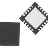
C8051F336-GMR Silicon Laboratories Inc, C8051F336-GMR Datasheet - Page 131

C8051F336-GMR
Manufacturer Part Number
C8051F336-GMR
Description
Microcontrollers (MCU) 16KB 10ADC 10DAC 768Ram MCU Lead Free
Manufacturer
Silicon Laboratories Inc
Datasheet
1.C8051F336-GM.pdf
(226 pages)
Specifications of C8051F336-GMR
Processor Series
C8051F3x
Core
8051
Data Bus Width
8 bit
Program Memory Type
Flash
Program Memory Size
16 KB
Data Ram Size
768 B
Interface Type
I2C, SPI, UART
Maximum Clock Frequency
25 MHz
Number Of Programmable I/os
17
Number Of Timers
4
Operating Supply Voltage
2.7 V to 3.6 V
Maximum Operating Temperature
+ 85 C
Mounting Style
SMD/SMT
Package / Case
QFN-20
3rd Party Development Tools
KSK-SL-TOOLSTICK, PK51, CA51, A51, ULINK2
Development Tools By Supplier
C8051F336DK
Minimum Operating Temperature
- 40 C
On-chip Adc
10 bit
On-chip Dac
10 bit
Package
20QFN
Device Core
8051
Family Name
C8051F336
Maximum Speed
25 MHz
Ram Size
768 Byte
Operating Temperature
-40 to 85 °C
Lead Free Status / Rohs Status
Details
Available stocks
Company
Part Number
Manufacturer
Quantity
Price
Company:
Part Number:
C8051F336-GMR
Manufacturer:
SILICON
Quantity:
100
Part Number:
C8051F336-GMR
Manufacturer:
SILICON LABS/芯科
Quantity:
20 000
Company:
Part Number:
C8051F336-GMR
Manufacturer:
SILICON
Quantity:
13 282
SFR Definition 20.6. P1MAT: Port 1 Match Register
SFR Address = 0xED
20.6. Special Function Registers for Accessing and Configuring Port I/O
All Port I/O are accessed through corresponding special function registers (SFRs) that are both byte
addressable and bit addressable. When writing to a Port, the value written to the SFR is latched to
maintain the output data value at each pin. When reading, the logic levels of the Port's input pins are
returned regardless of the XBRn settings (i.e., even when the pin is assigned to another signal by the
Crossbar, the Port register can always read its corresponding Port I/O pin). The exception to this is the
execution of the read-modify-write instructions that target a Port Latch register as the destination. The
read-modify-write instructions when operating on a Port SFR are the following: ANL, ORL, XRL, JBC, CPL,
INC, DEC, DJNZ and MOV, CLR or SETB, when the destination is an individual bit in a Port SFR. For
these instructions, the value of the latch register (not the pin) is read, modified, and written back to the
SFR.
Each Port has a corresponding PnSKIP register which allows its individual Port pins to be assigned to
digital functions or skipped by the Crossbar. All Port pins used for analog functions, GPIO, or dedicated
digital functions such as the EMIF should have their PnSKIP bit set to ‘1’.
The Port input mode of the I/O pins is defined using the Port Input Mode registers (PnMDIN). Each Port
cell can be configured for analog or digital I/O. This selection is required even for the digital resources
selected in the XBRn registers, and is not automatic. The only exception to this is P2.4, which can only be
used for digital I/O.
The output driver characteristics of the I/O pins are defined using the Port Output Mode registers (PnMD-
OUT). Each Port Output driver can be configured as either open drain or push-pull. This selection is
required even for the digital resources selected in the XBRn registers, and is not automatic. The only
exception to this is the SMBus (SDA, SCL) pins, which are configured as open-drain regardless of the
PnMDOUT settings.
Name
Reset
Bit
7:0
Type
Bit
P1MAT[7:0]
Name
7
1
Port 1 Match Value.
Match comparison value used on Port 1 for bits in P1MASK which are set to ‘1’.
0: P1.n pin logic value is compared with logic LOW.
1: P1.n pin logic value is compared with logic HIGH.
6
1
5
1
Rev.1.0
4
1
P1MAT[7:0]
R/W
Function
3
1
C8051F336/7/8/9
2
1
1
1
0
1
131


