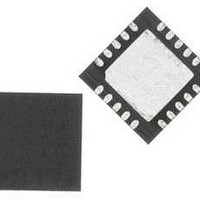
C8051F336-GMR Silicon Laboratories Inc, C8051F336-GMR Datasheet - Page 73

C8051F336-GMR
Manufacturer Part Number
C8051F336-GMR
Description
Microcontrollers (MCU) 16KB 10ADC 10DAC 768Ram MCU Lead Free
Manufacturer
Silicon Laboratories Inc
Datasheet
1.C8051F336-GM.pdf
(226 pages)
Specifications of C8051F336-GMR
Processor Series
C8051F3x
Core
8051
Data Bus Width
8 bit
Program Memory Type
Flash
Program Memory Size
16 KB
Data Ram Size
768 B
Interface Type
I2C, SPI, UART
Maximum Clock Frequency
25 MHz
Number Of Programmable I/os
17
Number Of Timers
4
Operating Supply Voltage
2.7 V to 3.6 V
Maximum Operating Temperature
+ 85 C
Mounting Style
SMD/SMT
Package / Case
QFN-20
3rd Party Development Tools
KSK-SL-TOOLSTICK, PK51, CA51, A51, ULINK2
Development Tools By Supplier
C8051F336DK
Minimum Operating Temperature
- 40 C
On-chip Adc
10 bit
On-chip Dac
10 bit
Package
20QFN
Device Core
8051
Family Name
C8051F336
Maximum Speed
25 MHz
Ram Size
768 Byte
Operating Temperature
-40 to 85 °C
Lead Free Status / Rohs Status
Details
Available stocks
Company
Part Number
Manufacturer
Quantity
Price
Company:
Part Number:
C8051F336-GMR
Manufacturer:
SILICON
Quantity:
100
Part Number:
C8051F336-GMR
Manufacturer:
SILICON LABS/芯科
Quantity:
20 000
Company:
Part Number:
C8051F336-GMR
Manufacturer:
SILICON
Quantity:
13 282
- Current page: 73 of 226
- Download datasheet (2Mb)
SFR Definition 12.6. PSW: Program Status Word
SFR Address = 0xD0; Bit-Addressable
Name
Reset
Bit
4:3
Type
7
6
5
2
1
0
Bit
PARITY
RS[1:0]
Name
CY
AC
OV
F0
F1
R/W
CY
7
0
Carry Flag.
This bit is set when the last arithmetic operation resulted in a carry (addition) or a bor-
row (subtraction). It is cleared to logic 0 by all other arithmetic operations.
Auxiliary Carry Flag.
This bit is set when the last arithmetic operation resulted in a carry into (addition) or a
borrow from (subtraction) the high order nibble. It is cleared to logic 0 by all other arith-
metic operations.
User Flag 0.
This is a bit-addressable, general purpose flag for use under software control.
Register Bank Select.
These bits select which register bank is used during register accesses.
00: Bank 0, Addresses 0x00-0x07
01: Bank 1, Addresses 0x08-0x0F
10: Bank 2, Addresses 0x10-0x17
11: Bank 3, Addresses 0x18-0x1F
Overflow Flag.
This bit is set to 1 under the following circumstances:
The OV bit is cleared to 0 by the ADD, ADDC, SUBB, MUL, and DIV instructions in all
other cases.
User Flag 1.
This is a bit-addressable, general purpose flag for use under software control.
Parity Flag.
This bit is set to logic 1 if the sum of the eight bits in the accumulator is odd and cleared
if the sum is even.
An ADD, ADDC, or SUBB instruction causes a sign-change overflow.
A MUL instruction results in an overflow (result is greater than 255).
A DIV instruction causes a divide-by-zero condition.
R/W
AC
6
0
R/W
F0
5
0
Rev.1.0
4
0
RS[1:0]
R/W
Function
3
0
C8051F336/7/8/9
R/W
OV
2
0
R/W
F1
1
0
PARITY
R
0
0
73
Related parts for C8051F336-GMR
Image
Part Number
Description
Manufacturer
Datasheet
Request
R
Part Number:
Description:
SMD/C°/SINGLE-ENDED OUTPUT SILICON OSCILLATOR
Manufacturer:
Silicon Laboratories Inc
Part Number:
Description:
Manufacturer:
Silicon Laboratories Inc
Datasheet:
Part Number:
Description:
N/A N/A/SI4010 AES KEYFOB DEMO WITH LCD RX
Manufacturer:
Silicon Laboratories Inc
Datasheet:
Part Number:
Description:
N/A N/A/SI4010 SIMPLIFIED KEY FOB DEMO WITH LED RX
Manufacturer:
Silicon Laboratories Inc
Datasheet:
Part Number:
Description:
N/A/-40 TO 85 OC/EZLINK MODULE; F930/4432 HIGH BAND (REV E/B1)
Manufacturer:
Silicon Laboratories Inc
Part Number:
Description:
EZLink Module; F930/4432 Low Band (rev e/B1)
Manufacturer:
Silicon Laboratories Inc
Part Number:
Description:
I°/4460 10 DBM RADIO TEST CARD 434 MHZ
Manufacturer:
Silicon Laboratories Inc
Part Number:
Description:
I°/4461 14 DBM RADIO TEST CARD 868 MHZ
Manufacturer:
Silicon Laboratories Inc
Part Number:
Description:
I°/4463 20 DBM RFSWITCH RADIO TEST CARD 460 MHZ
Manufacturer:
Silicon Laboratories Inc
Part Number:
Description:
I°/4463 20 DBM RADIO TEST CARD 868 MHZ
Manufacturer:
Silicon Laboratories Inc
Part Number:
Description:
I°/4463 27 DBM RADIO TEST CARD 868 MHZ
Manufacturer:
Silicon Laboratories Inc
Part Number:
Description:
I°/4463 SKYWORKS 30 DBM RADIO TEST CARD 915 MHZ
Manufacturer:
Silicon Laboratories Inc
Part Number:
Description:
N/A N/A/-40 TO 85 OC/4463 RFMD 30 DBM RADIO TEST CARD 915 MHZ
Manufacturer:
Silicon Laboratories Inc
Part Number:
Description:
I°/4463 20 DBM RADIO TEST CARD 169 MHZ
Manufacturer:
Silicon Laboratories Inc


