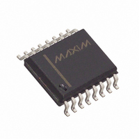
MAX532BCWE Maxim Integrated Products, MAX532BCWE Datasheet

MAX532BCWE
Specifications of MAX532BCWE
Available stocks
Related parts for MAX532BCWE
MAX532BCWE Summary of contents
Page 1
... Information PART TEMP. RANGE PIN-PACKAGE MAX532ACPE 0°C to +70°C MAX532BCPE 0°C to +70°C MAX532ACWE 0°C to +70°C MAX532BCWE 0°C to +70°C MAX532BC/D 0°C to +70°C Ordering Information continued on last page. * Contact factory for dice specifications. __________________Pin Configuration RFBA TOP VIEW ...
Page 2
Dual, Serial-Input, Voltage-Output, 12-Bit MDAC ABSOLUTE MAXIMUM RATINGS Pin Voltages V to DGND, AGNDA, AGNDB........................-0.3V to +17V DGND, AGNDA, AGNDB (Note 1) ..........+0.3V to -17V SS VREFA, VREFB.............................(V - 0.3V AGNDA, AGNDB .....................(DGND - ...
Page 3
ELECTRICAL CHARACTERISTICS (continued 11.4V to 16.5V -11.4V to -16.5V, AGNDA = AGNDB = DGND = 0V, VREFA and VREFB = +10V VOUT_ connected to RFB_ MIN MAX ...
Page 4
Dual, Serial-Input, Voltage-Output, 12-Bit MDAC ELECTRICAL CHARACTERISTICS (continued 11.4V to 16.5V -11.4V to -16.5V, AGNDA = AGNDB = DGND = 0V, VREFA and VREFB = +10V VOUT_ connected to RFB_ ...
Page 5
Operating Characteristics (V = 15V -15V 2kΩ 100pF, unless otherwise noted OUTPUT VOLTAGE SWING vs. RESISTIVE LOAD 25 VREF = 20V at 1kHz p ...
Page 6
Dual, Serial-Input, Voltage-Output, 12-Bit MDAC ____________________________Typical Operating Characteristics (continued 15V -15V 2kΩ 100pF, unless otherwise noted SMALL-SIGNAL PULSE RESPONSE AGNDA 50mV/div OUTA TIMEBASE = ...
Page 7
Diagrams CS t CSHO t t CSSO CH SCLK DIN DOUT LDAC Figure 1. Timing Diagram _______________________________________________________________________________________ Dual, Serial-Input, Voltage-Output, 12-Bit MDAC D23 Q1 Q23 ...
Page 8
Dual, Serial-Input, Voltage-Output, 12-Bit MDAC _______________________________________________Timing Diagrams (continued) CS SCLK DIN D23 D16 ............................................ MSB DACB DOUT Q23 Q22 ..................................... Q16 MSB DACB FROM PREVIOUS WRITE Figure 2. 3-Wire Interface Timing Diagram (LDAC = DGND) CS SCLK DIN D23 D16 ...
Page 9
SCLK SK DIN SO MAX532 DOUT SI CS I/O LDAC I/O THE DOUT-SI CONNECTION IS NOT REQUIRED FOR WRITING TO THE MAX532, BUT MAY BE USED FOR READ-BACK PURPOSES. Figure 4. Connections for Microwire _______________Detailed Description Digital Interface ...
Page 10
Dual, Serial-Input, Voltage-Output, 12-Bit MDAC MAX532 SCLK SCLK DIN DOUT DIN CS CS LDAC MAX532 SCLK SCLK DIN DIN CS CS LDAC Figure 6. Daisy-chained or individual MAX532s are simultaneously updated by bringing CS high when using the 3-wire interface ...
Page 11
Table 1. t Delay Times RC V (V) C (pF) R (kΩ) PULL- 4.5 100 1 4.5 150 11.4 100 ...
Page 12
Dual, Serial-Input, Voltage-Output, 12-Bit MDAC Output Amplifiers The output amplifiers are stable with any combination of resistive loads ≥ 2kΩ and capacitive loads ≤ 100pF. They are internally compensated, and settle to ±0.01% FSR (1/2LSB) in 2.5µs. Unipolar Configuration Figure ...
Page 13
MAX532 DACA R 4096 2 CODE R/2 RFBA AGNDA 4 Figure 12. Programmable-Gain Amplifer ______________________________________________________________________________________ Dual, Serial-Input, Voltage-Output, 12-Bit MDAC Programmable-Gain Amplifier (PGA) The DAC/amplifier combination, along with access to the feedback resistors, makes the MAX532 ideal ...
Page 14
Dual, Serial-Input, Voltage-Output, 12-Bit MDAC __Ordering Information (continued) PART TEMP. RANGE PIN-PACKAGE MAX532AEPE -40°C to +85°C 16 Plastic DIP MAX532BEPE -40°C to +85°C 16 Plastic DIP MAX532AEWE -40°C to +85°C 16 Wide SO MAX532BEWE -40°C to +85°C 16 Wide SO ...
Page 15
Information ______________________________________________________________________________________ Dual, Serial-Input, Voltage-Output, 12-Bit MDAC 45˚ 0.127mm 0.004in INCHES ...
Page 16
... Maxim cannot assume responsibility for use of any circuitry other than circuitry entirely embodied in a Maxim product. No circuit patent licenses are implied. Maxim reserves the right to change the circuitry and specifications without notice at any time. 16 ____________________________Maxim Integrated Products, 120 San Gabriel Drive, Sunnyvale, CA 94086 (408) 737-7600 © 1994 Maxim Integrated Products Printed USA is a registered trademark of Maxim Integrated Products ...


