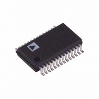
AD5554BRS Analog Devices Inc, AD5554BRS Datasheet

AD5554BRS
Specifications of AD5554BRS
Available stocks
Related parts for AD5554BRS
AD5554BRS Summary of contents
Page 1
FEATURES AD5544: 16-bit resolution INL of ±1 LSB (B Grade) INL of ±2 LSB (A Grade) AD5554: 14-bit resolution INL of ±0.5 LSB (B Grade full-scale current ± 20%, with V REF 0.9 μs settling time to ±0.1% ...
Page 2
AD5544/AD5554 TABLE OF CONTENTS Features .............................................................................................. 1 Applications ....................................................................................... 1 General Description ......................................................................... 1 Functional Block Diagram .............................................................. 1 Revision History ............................................................................... 2 Specifications ..................................................................................... 3 AD5544 Electrical Characteristics ............................................. 3 AD5554 Electrical Characteristics ............................................. 4 Timing Diagrams .......................................................................... 5 ...
Page 3
SPECIFICATIONS AD5544 ELECTRICAL CHARACTERISTICS virtual GND OUT range of −40°C to +125°C, unless otherwise noted. Table 1. Parameter Symbol 1 STATIC PERFORMANCE Resolution ...
Page 4
AD5544/AD5554 Parameter Symbol 4 AC CHARACTERISTICS Output Voltage Settling Time t S Reference Multiplying BW BW − DAC Glitch Impulse Q Feedthrough Error V x/V OUT Crosstalk Error V A/V OUT Digital Feedthrough Q Total Harmonic Distortion THD ...
Page 5
Parameter Symbol Data Setup t DS Data Hold t DH Load Setup t LDS Load Hold t LDH SUPPLY CHARACTERISTICS Power Supply Range V DD RANGE Positive Supply Current I DD Negative Supply Current I SS Power Dissipation P DISS ...
Page 6
AD5544/AD5554 ABSOLUTE MAXIMUM RATINGS Table 3. Parameter V to GND GND GND REF Logic Input and Output to GND V GND OUT DGND GND Input Current to Any Pin ...
Page 7
PIN CONFIGURATION AND FUNCTION DESCRIPTIONS Table 4. Pin Function Descriptions Pin No. Mnemonic Description DAC A Analog Ground. GND DAC A Current Output. OUT DAC A Reference Voltage Input Terminal. Establishes ...
Page 8
AD5544/AD5554 TYPICAL PERFORMANCE CHARACTERISTICS 0.10 0.05 0 –0.05 –0.10 –0.15 –0.20 –0.25 –0.30 –0.35 –0.40 0 10,000 20,000 30,000 40,000 CODE Figure 6. AD5544 DNL vs. Code, T 0.20 0.15 0.10 0.05 0 –0.05 –0.10 –0.15 –0.20 0 2000 4000 ...
Page 9
TIME (µs) Figure 12. AD5544 Midscale Transition 10V REF Figure 13. AD5544 Large Signal Settling Time 0.1 ...
Page 10
AD5544/AD5554 THEORY OF OPERATION The AD5544 and the AD5554 contain four 16-bit and 14-bit, current output DACs, respectively. Each DAC has its own inde- pendent multiplying reference input. Both the AD5544 and the AD5554 use a 3-wire, SPI-compatible serial data ...
Page 11
REF FROM OTHER DACS A GND V SS DIGITAL INTERFACE CONNECTIONS OMITTED. FOR CLARITY SWITCHES S1 AND S2 ARE CLOSED, V MUST BE POWERED. DD Figure 20. Recommended Kelvin-Sensed Hookup Rev. ...
Page 12
AD5544/AD5554 SERIAL DATA INTERFACE The AD5544/AD5554 use a 3-wire ( CS , SDI, CLK), SPI-compatible serial data interface. Serial data of the AD5544/AD5554 is clocked into the serial input register in an 18-bit and 16-bit data-word format, respectively. The MSB ...
Page 13
TRUTH TABLES 1 Table 8. AD5544 Control Logic Truth Table CS LDAC RS CLK MSB High X High High X Low Low High High X Low ↑ High High Low High High High X ↑ Low High ...
Page 14
AD5544/AD5554 CS EN CLK SDI D10 D11 D12 D13 D14 DAC A SDO D15 2:4 DECODE DGND TO INPUT REGISTER CS EN SHIFT REGISTER ...
Page 15
Layout and Power Supply Bypassing It is good practice to employ a compact, minimum lead length layout design. The leads to the input should be as direct as possible with a minimum conductor length. Ground paths should have low resistance ...
Page 16
... AD5544ARSZ 1 16 ±2 1 AD5544ARSZ-REEL7 16 ±2 1 AD5544BRSZ 16 ±1 1 AD5544BRSZ-REEL7 16 ± ±0.5 AD5554BRSZ RoHS Compliant Part. ©2000–2009 Analog Devices, Inc. All rights reserved. Trademarks and registered trademarks are the property of their respective owners. 10.50 10.20 9. 5.60 5.30 8.20 5.00 7.80 7. 1.85 1.75 1 ...


