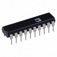
AD7112CN Analog Devices Inc, AD7112CN Datasheet

AD7112CN
Specifications of AD7112CN
Related parts for AD7112CN
AD7112CN Summary of contents
Page 1
...
Page 2
AD7112–SPECIFICATIONS Output amplifier AD712 except where noted. All specifications T C Version Parameter +25 C ACCURACY Resolution 0.375 Accuracy Relative Attenuation 0.375 dB Steps: Accuracy 0. Monotonic ...
Page 3
TIMING SPECIFICATIONS Parameter Setup Time Hold Time t DAC Select to WR Setup Time t DAC Select to WR Hold Time t Data Valid to WR Setup Time t Data Valid to ...
Page 4
... Glitch im- pulse is measured with V = AGND. IN ORDERING INFORMATION Specified Temperature Accuracy Model Range Range AD7112BN – + AD7112CN – + AD7112BR – + AD7112CR – + Plastic DIP SOIC. Lead Temperature (Soldering, 10 secs +300 C Power Dissipation, SOIC . . . . . . . . . . . . . . . . . . . . . . . . . 0 Thermal Impedance . . . . . . . . . . . . . . . . . . . . . . 75 C/W ...
Page 5
CIRCUIT DESCRIPTION GENERAL CIRCUIT INFORMATION The AD7112 consists of a dual 17-bit R-2R CMOS multiplying D/A converter with extensive digital logic. Figure 1 shows a sim- plified circuit of the D/A converter section of the AD7112. The logic translates the ...
Page 6
AD7112 INTERFACE LOGIC INFORMATION DAC Selection Both DAC latches share a common 8-bit port. The control in- put DAC A/DAC B selects which DAC can accept data from the input port. Mode Selection Inputs CS and WR control the operating ...
Page 7
Another error arises from the output amplifier’s input offset volt- age. The amplifier is operated with a fixed feedback resistance, but the equivalent source impedance (the AD7112 output im- pedance) varies as a function of the attenuation level. This has ...
Page 8
AD7112 – rms IN INPUT CODE = 0000 0000 ° +25 C – 15pF –80 –90 –100 FREQUENCY – Hz Figure 8. Distortion vs. Frequency –40 V ...
Page 9
V = +5V DD ° –0.2 –0.4 ...
Page 10
AD7112 MICROPROCESSOR INTERFACING Figures show interfaces between the AD7112 and three popular 8-bit microprocessor systems, the MC68008, 8085A/8088 and the 8051. In the MC68008 and 8085/8088 in- terfaces, the AD7112 is memory mapped with separate ad- dresses ...
Page 11
VARIABLE INPUT GAIN ELEMENT 1/2 AD7112 DETECTOR UP/DOWN COUNTER D U COMPARATOR END STOP AND CONTROL LOGIC Figure 21. Automatic Gain Control System Programmable State Variable Filter The AD7112 with its multiplying capability and fast settling time is ideal for ...
Page 12
AD7112 PIN 1 0.210 (5.33) MAX 0.160 (4.06) 0.115 (2.93) PIN 1 0.0118 (0.30) 0.0040 (0.10) OUTLINE DIMENSIONS Dimensions shown in inches and (mm). 20-Pin Plastic DIP (N-20 0.280 (7.11) 0.240 (6.10 0.325 (8.25) 1.060 (26.90) ...


