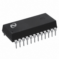
DAC1210LCJ National Semiconductor, DAC1210LCJ Datasheet - Page 12

DAC1210LCJ
Manufacturer Part Number
DAC1210LCJ
Description
IC DAC 12BIT MPU 24-DIP
Manufacturer
National Semiconductor
Series
MICRO-DAC™r
Datasheet
1.DAC1210LCJ.pdf
(18 pages)
Specifications of DAC1210LCJ
Settling Time
1µs
Number Of Bits
12
Data Interface
Parallel
Number Of Converters
1
Voltage Supply Source
Single Supply
Power Dissipation (max)
500mW
Operating Temperature
-40°C ~ 85°C
Mounting Type
Through Hole
Package / Case
*
Case
DIP-24L
Lead Free Status / RoHS Status
Contains lead / RoHS non-compliant
Other names
*DAC1210LCJ
Available stocks
Company
Part Number
Manufacturer
Quantity
Price
Company:
Part Number:
DAC1210LCJ
Manufacturer:
NS
Quantity:
960
Company:
Part Number:
DAC1210LCJ
Manufacturer:
NS
Quantity:
960
Part Number:
DAC1210LCJ
Manufacturer:
NS/国半
Quantity:
20 000
Company:
Part Number:
DAC1210LCJ-1
Manufacturer:
NS
Quantity:
2 067
Application Hints
2 0 ANALOG APPLICATIONS
The analog output signal for these DACs is derived from a
conventional R-2R current switching ladder network A de-
tailed description of this network can be found on the
DAC1000 series data sheet Basically output I
vides a current directly proportional to the product of the
applied reference voltage and the digital input word A sec-
ond output I
plement of the digital input Specifically
where D is the decimal equivalent of the applied 12-bit bina-
ry word (ranging from 0 to 4095) V
plied to the V
the R-2R ladder R is nominally 15 k
2 1 Obtaining a Unipolar Output Voltage
To maintain linearity of output current with changes in the
applied digital code it is important that the voltages at both
of the current output pins be as near ground potential (0
V
ing at either I
error In most applications this output current is converted to
a voltage by using an op amp as shown in Figure 9
BI-FET
DC
I
I
OUT1
OUT2
) as possible With V
TM
is a trademark of National Semiconductor Corp
e
e
V
V
OUT2
REF
REF
R
R
REF
OUT1
c
c
terminal and R is the internal resistance of
will be a current proportional to the com-
4096
4095
or I
D
4096
OUT2
REF
b
D
e a
(Continued)
will cause a 0 01% linearity
10V every millivolt appear-
REF
is the voltage ap-
FIGURE 9 Unipolar Output Configuration
OUT1
pro-
V
for 0
OUT
s
e
e b
12
D
b
s
(I
V
4096
OUT1 c
REF
4095
The inverting input of the op amp is a virtual ground created
by the feedback from its output through the internal 15 k
resistor R
digital input and the reference voltage) will flow through R
to the output of the amplifier Two-quadrant operation can
be obtained by reversing the polarity of V
I
of the amplifier The output voltage in either case is always
equal to I
erence voltage
The reference can be either a stable DC voltage source or
an AC signal anywhere in the range from
The DAC can be thought of as a digitally controlled attenua-
tor the output voltage is always less than the applied refer-
ence voltage The V
nominal impedance of 15 k
Always use the internal R
voltage since this resistor matches (and tracks with temper-
ature) the value of the resistors used to generate the output
current (I
The selected op amp should have as low a value of input
bias current as possible The product of the bias current
times the feedback resistance creates an output voltage er-
ror which can be significant in low reference voltage appli-
cations BI-FET
with these DACs because of their very low input current
OUT1
(D)
R
to flow into the DAC and be sourced from the output
Fb
)
OUT1
OUT1 c
Fb
)
All of the output current (determined by the
TM
R
Fb
op amps are highly recommended for use
REF
and is the opposite polarity of the ref-
terminal of the device presents a
Fb
to ground to external circuitry
resistor to create an output
REF
b
TL H 5690 – 15
10V to
thus causing
a
10V
Fb


