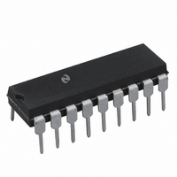
DAC1220LCN National Semiconductor, DAC1220LCN Datasheet - Page 3

DAC1220LCN
Manufacturer Part Number
DAC1220LCN
Description
IC DAC 12BIT BINARY 18-DIP
Manufacturer
National Semiconductor
Datasheet
1.DAC1021LCN.pdf
(14 pages)
Specifications of DAC1220LCN
Settling Time
500ns
Number Of Bits
12
Number Of Converters
1
Power Dissipation (max)
30mW
Operating Temperature
0°C ~ 70°C
Mounting Type
Through Hole
Package / Case
*
Lead Free Status / RoHS Status
Contains lead / RoHS non-compliant
Data Interface
-
Voltage Supply Source
-
Other names
*DAC1220LCN
Available stocks
Company
Part Number
Manufacturer
Quantity
Price
Part Number:
DAC1220LCN
Manufacturer:
NS/国半
Quantity:
20 000
Digital Input
Digital Input Current
Supply Current
Operating Power Supply
Range
Electrical Characteristics
Note 1 V
linearity error For instance if the linearity error at 25 C is 0 045% FS it could increase to 0 054% at 70 C and the DAC will be no longer a 10-bit part Note
however that the linearity error is specified over the device full temperature range which is a more stringent specification since it includes the linearity error
temperature coefficient
Note 2 Using internal feedback resistor as shown in Figure 3
Note 3 Both I
0 005% linearity error will be introduced
Note 4 Human body model 100 pF discharged through a 1 5 k
Note 5 Absolute Maximum Ratings indicate limits beyond which damage to the device may occur DC and AC electrical specifications do not apply when operating
the device beyond its specified operating conditions
Note 6 The maximum power dissipation must be derated at elevated temperatures and is dictated by T
allowable power dissipation at any temperature is P
device T
120 C W for the N16 this number is 125 C W and for the V20 this number is 95 C W
Typical Performance Characteristics
Low Threshold
High Threshold
Parameter
JMAX
REF
e
OUT 1
e
FIGURE 1 Digital Input Threshold vs
g
125 C and the typical junction-to-ambient thermal resistance of the J18 package when board mounted is 85 C W For the N18 package
10V and V
and I
Ambient Temperature
OUT 2
REF
must go to ground or the virtual ground of an operational amplifier If V
e
g
(Figure 1)
(Figures 1 and 2)
1V A linearity error temperature coefficient of 0 0002% FS for a 45 C rise only guarantees 0 009% maximum change in
T
T
T
Digital Input High
Digital Input Low
All Digital Inputs High
All Digital Inputs Low
MIN k
MIN k
MIN s
Conditions
T
T
T
A k
A k
A s
D
T
T
T
e
MAX
MAX
MAX
(V
(T
a
JMAX
e
15V V
b
resistor
T
A
)
Min
2 4
REF
5
JA
DAC1020 DAC1021
or the number given in the Absolute Maximum Ratings whichever is lower For this
e
3
10 000V T
DAC1022
b
Typ
0 2
0 6
1
50
FIGURE 2 Gain Error Variation vs V
A
b
e
Max
100
0 8
1 6
15
200
2
25 C unless otherwise specified) (Continued)
JMAX
REF
e
10V every millivolt offset between I
JA
Min
2 4
and the ambient temepature T
5
DAC1220 DAC1222
b
Typ
0 2
0 6
1
50
b
http
Max
100
0 8
1 6
15
200
2
a
A
OUT 1
www national com
The maximum
TL H 5689– 2
or I
Units
OUT 2
mA
mA
JA
V
V
V
A
A
is


