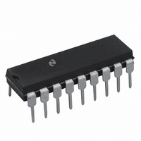
DAC1220LCN National Semiconductor, DAC1220LCN Datasheet - Page 4

DAC1220LCN
Manufacturer Part Number
DAC1220LCN
Description
IC DAC 12BIT BINARY 18-DIP
Manufacturer
National Semiconductor
Datasheet
1.DAC1021LCN.pdf
(14 pages)
Specifications of DAC1220LCN
Settling Time
500ns
Number Of Bits
12
Number Of Converters
1
Power Dissipation (max)
30mW
Operating Temperature
0°C ~ 70°C
Mounting Type
Through Hole
Package / Case
*
Lead Free Status / RoHS Status
Contains lead / RoHS non-compliant
Data Interface
-
Voltage Supply Source
-
Other names
*DAC1220LCN
Available stocks
Company
Part Number
Manufacturer
Quantity
Price
Part Number:
DAC1220LCN
Manufacturer:
NS/国半
Quantity:
20 000
http
Typical Applications
The following applications are also valid for 12-bit systems
using the DAC1220 and 2 additional digital inputs
Operational Amplifier Bias Current ( Figure 3 )
The op amp bias current I
feedback resistor BI-FET op amps have low I
fore the 15k
strongly recommended for the DAC1020 applications
V
The output impedance R
the digital input code which causes a modulation of the op-
erational amplifier output offset It is therefore recommend-
ed to adjust the op amp V
digital inputs are high R
is high and R
OS
www national com
Op Amp Family
Considerations
LM741
LF357
LF356
LF351
c
OUT
I
b
error they introduce is negligible they are
approaches infinity if all inputs are low
OUT
OUT
OS
b
SELECTING AND COMPENSATING THE OPERATIONAL AMPLIFIER
10 pF
22 pF
24 pF
0
is E 45k if a single digital input
flows through the 15k internal
FIGURE 3 Basic Connection Unipolar or 2-Quadrant Multiplying
C
R
of the DAC is modulated by
F
OUT
is E 15k if more than 4
2 4k
V
0
where A
b
R
%
%
%
OUT
Configuration (Digital Attenuator)
s
10V
i
b
V
and there-
OUT s
e b
A
s
N
N
V
e
e
V
REF s
REF
b
0 if the A
1 if the A
1023
1024
25k
25k
10k
10k
10V
A1
P
2
V
a
N
REF
N
4
digital input is low
A2
digital input is high
4
a
Operational Amplifier V
Connect all digital inputs A1– A10 to ground and adjust the
potentiometer to bring the op amp V
mV from ground potential If V
V
lution of the V
resistor between the inverting input of the op amp to
ground After V
Full-Scale Adjust ( Figure 4 )
Switch high all the digital inputs A1– A10 and measure the
op amp output voltage Use a 500
shown to bring
1023 1024
OS
A3
8
a
adjustment is required It is helpful to increase the reso-
V
V
V
V
V
W
a
a
b
b
1024
A10
OS
OS
ll
Circuit Settling
adjust procedure by connecting a 1 k
has been adjusted remove the 1 k
V
OUT
Time t
1 5 s
40 s
3 s
4 s
ll
OS
to a voltage equal to V
Adjust ( Figure 3 )
s
REF
is less than 10V a finer
OUT
potentiometer as
pin to within
TL H 5689 – 3
Circuit Small
Signal BW
200 kHz
0 5M
0 5M
1M
REF c
g
1


