DAC1222LCN National Semiconductor, DAC1222LCN Datasheet - Page 10
DAC1222LCN
Manufacturer Part Number
DAC1222LCN
Description
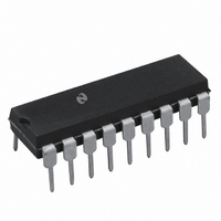
IC DAC 12BIT BINARY 18-DIP
Manufacturer
National Semiconductor
Datasheet
1.DAC1021LCN.pdf
(14 pages)
Specifications of DAC1222LCN
Settling Time
500ns
Number Of Bits
12
Number Of Converters
1
Power Dissipation (max)
30mW
Operating Temperature
0°C ~ 70°C
Mounting Type
Through Hole
Package / Case
*
Lead Free Status / RoHS Status
Contains lead / RoHS non-compliant
Data Interface
-
Voltage Supply Source
-
Other names
*DAC1222LCN


http
D A transfer characteristic It is measured after calibrating
Definition of Terms
Resolution Resolution is defined as the reciprocal of the
number of discrete steps in the D A output It is directly
related to the number of switches or bits within the D A For
example the DAC1020 has 2
DAC1220 has 2
has 10-bit resolution while the DAC1220 has 12-bit resolu-
tion
Linearity Error Linearity error is the maximum deviation
from a straight line passing through the endpoints of the
for zero (see V
scale Linearity error is a design parameter intrinsic to the
device and cannot be externally adjusted
(a) End point test after zero and full-scale adjust
Note (a) (b1) and (b2) above illustrate the difference between ‘‘end point’’ National’s linearity test (a) and ‘‘best straight line’’ test Note that both devices in (a) and
(b2) meet the
Connection Diagrams
www national com
The DAC has 1 LSB linearity error
Dual-In-Line Package
g
DAC102X
LSB linearity error specification but the end point test is a more ‘‘real life’’ way of characterizing the DAC
12
OS
a
or 4096 steps Therefore the DAC1020
adjust in typical applications) and full-
TL H 5689– 13
10
or 1024 steps while the
PLCC Package
DAC1020
b1
10
Power Supply Sensitivity Power supply sensitivity is a
measure of the effect of power supply changes on the D A
full-scale output
Settling Time Full-scale settling time requires a zero to full-
scale or full-scale to zero output change Settling time is the
time required from a code transition until the D A output
reaches within
Full-Scale Error Full-scale error is a measure of the output
error between an ideal D A and the actual device output
Ideally for the DAC1020 full-scale is V
V
LE
justable to zero as shown in Figure 5
(b) By shifting the full-scale calibration on of the DAC of
REF
e
Figure (b1) we could pass the ‘‘best straight line’’ (b2)
test and meet the
TL H 5689 – 12
10 0000V 9 8 mV
e
10V
g
and
LSB of final output value
g
unipolar
e
9 9902V Full-scale error is ad-
linearity error specification
Dual-In-Line Package
operation
DAC122X
b2
REF
b
1 LSB For
V
TL H 5689 – 10
TL H 5689 – 11
FULL-SCA-
Related parts for DAC1222LCN
Image
Part Number
Description
Manufacturer
Datasheet
Request
R

Part Number:
Description:
National Semiconductor [8-Bit D/A Converter]
Manufacturer:
National Semiconductor
Datasheet:
Part Number:
Description:
National Semiconductor [Media Coprocessor]
Manufacturer:
National Semiconductor
Datasheet:
Part Number:
Description:
Digitally Controlled Tone and Volume Circuit with Stereo Audio Power Amplifier, Microphone Preamp Stage and National 3D Sound
Manufacturer:
National Semiconductor
Datasheet:
Part Number:
Description:
Digitally Controlled Tone and Volume Circuit with Stereo Audio Power Amplifier, Microphone Preamp Stage and National 3D Sound
Manufacturer:
National Semiconductor
Datasheet:
Part Number:
Description:
AC97 Rev 2 Codec with Sample Rate Conversion and National 3D Sound
Manufacturer:
National Semiconductor
Part Number:
Description:
Manufacturer:
National Semiconductor
Datasheet:
Part Number:
Description:
Manufacturer:
National Semiconductor
Datasheet:
Part Number:
Description:
General Purpose, Low Voltage, Low Power, Rail-to-Rail Output Operational Amplifiers
Manufacturer:
National Semiconductor
Datasheet:
Part Number:
Description:
8-bit 20 MSPS flash A/D converter.
Manufacturer:
National Semiconductor
Datasheet:
Part Number:
Description:
Low Noise Quad Operational Amplifier
Manufacturer:
National Semiconductor
Datasheet:
Part Number:
Description:
Quad Differential Line Receivers
Manufacturer:
National Semiconductor
Datasheet:
Part Number:
Description:
Quad High Speed Trapezoidal? Bus Transceiver
Manufacturer:
National Semiconductor
Datasheet:
Part Number:
Description:
Dual Line Receiver
Manufacturer:
National Semiconductor
Datasheet:
Part Number:
Description:
TTL to 10k ECL Level Translator with Latch
Manufacturer:
National Semiconductor
Datasheet: