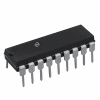
DAC1222LCN National Semiconductor, DAC1222LCN Datasheet - Page 6

DAC1222LCN
Manufacturer Part Number
DAC1222LCN
Description
IC DAC 12BIT BINARY 18-DIP
Manufacturer
National Semiconductor
Datasheet
1.DAC1021LCN.pdf
(14 pages)
Specifications of DAC1222LCN
Settling Time
500ns
Number Of Bits
12
Number Of Converters
1
Power Dissipation (max)
30mW
Operating Temperature
0°C ~ 70°C
Mounting Type
Through Hole
Package / Case
*
Lead Free Status / RoHS Status
Contains lead / RoHS non-compliant
Data Interface
-
Voltage Supply Source
-
Other names
*DAC1222LCN
http
V
where AN
Typical Applications
Operational Amplifiers V
a) Switch all the digital inputs high adjust the V
b) Switch the MSB high and the remaining digital inputs
OUT
FIGURE 8 Bipolar Configuration with a Single Op Amp
1
1
0
t
use LM336 for a voltage reference
www national com
s
e b
e
ometer of op amp B to bring its output to a value equal
to
low Adjust the V
its output value to within a 1 mV from ground potential
For V
mentioned in the previous application
AN
1
0
0
1 8 s
b
V
e a
e b
(V
1
0
0
REF
REF k
DIGITAL INPUT
REF
TRUE OFFSET BINARY OPERATION
1 if A
1 if A
1
0
0
A1
2
1024) (V)
N
1
0
0
a
N
10V a finer adjust is necessary as already
input is low
input is high
A2
4
1
0
0
OS
a
1
0
0
potentiometer of op amp A to bring
OS
1
0
0
a
Adjust ( Figure 7 )
1024
A10
1
0
0
FIGURE 7 Bipolar 4-Quadrant Multiplying Configuration
b
(Continued)
1
0
0
1024
1
V
REF c
b
TL H 5689– 5
V
V
OUT
1022 1024
0
REF
OS
potenti-
6
Gain Adjust (Full-Scale Adjust)
Assuming that the external 10k resistors are matched to
better than 0 1% the gain adjust of the circuit is the same
with the one previously discussed
R4
R3
Example V
Then R4
R3
e
a
Note that
e
0 0 0 0 0 0 0 0 0 0
0 0 0 0 0 0 0 0 0 1 V
0 1 1 1 1 1 1 1 1 1
1 0 0 0 0 0 0 0 0 0
1 0 0 0 0 0 0 0 0 1
1 1 1 1 1 1 1 1 1 1
(2A
R1
0 64R
By doubling the output range we get half the
resolution
The 10M resistor adds a 1 LSB ‘‘thump’’ to
allow full offset binary operation where the out-
put reaches zero for the half-scale code If
symmetrical output excursions are required
omit the 10M resistor
I
OUT 1
ll
FIGURE 9 Bipolar Configuration with
V
R2
e
COMPLEMENTARY OFFSET BINARY
b
DIGITAL INPUT
REF
9R R1
b
e
1) R
a
R A
e
Increased Output Swing
(BIPOLAR) OPERATION
2V V
I
OUT 2
V
e
R2
R1
b
0 8 R2 If R1
e
e
OUT
V
A
e
OUT(PEAK)
V
A
(swing) j
b
V
V
REF
R
b
b
LADDER
V
1
REF
e
R
b
0 2R then R2
g
b
e
REF c
V
V
10V A
V
REF
c
REF c
20k
REF c
a
V
V
(1022 1024)
1023
1024
b
V
OUT
1022 1024
0
REF
e
2 1024
e
2 1024
5V
0 25R
TL H 5689 – 6


