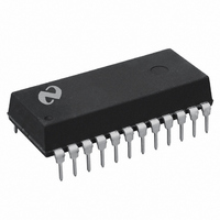
DAC1208LCJ National Semiconductor, DAC1208LCJ Datasheet - Page 10

DAC1208LCJ
Manufacturer Part Number
DAC1208LCJ
Description
IC DAC 12BIT DBL BUFF 24-DIP
Manufacturer
National Semiconductor
Series
MICRO-DAC™r
Datasheet
1.DAC1210LCJ.pdf
(18 pages)
Specifications of DAC1208LCJ
Settling Time
1µs
Number Of Bits
12
Data Interface
Parallel
Number Of Converters
1
Voltage Supply Source
Single Supply
Power Dissipation (max)
500mW
Operating Temperature
0°C ~ 70°C
Mounting Type
Through Hole
Package / Case
*
Case
DIP-24L
Lead Free Status / RoHS Status
Contains lead / RoHS non-compliant
Other names
*DAC1208LCJ
Available stocks
Company
Part Number
Manufacturer
Quantity
Price
Part Number:
DAC1208LCJ
Manufacturer:
NS/国半
Quantity:
20 000
Company:
Part Number:
DAC1208LCJ-1
Manufacturer:
ON
Quantity:
99
Application Hints
width If this does not provide a sufficient data hold time at
the end of the write cycle a negative edge triggered one-
shot can be included between the system write strobe and
the WR pin of the DAC This is illustrated in Figure 6 for an
exemplary system which provides a 250 ns WR strobe time
with a data hold time of only 10 ns
The proper data set-up time prior to the latching edge (low
to high transition) of the WR strobe is insured if the WR
pulse width is within spec and the data is valid on the bus for
the duration of the DAC WR strobe
1 9 Digital Signal Feedthrough
A typical microprocessor is a tremendous potential source
of high frequency noise which can be coupled to sensitive
analog circuitry The fast edges of the data and address bus
signals generate frequency components of 10’s of mega-
hertz and may cause fast transients to appear at the DAC
output even when data is latched internally
In low frequency or DC applications low pass filtering can
reduce the magnitude of any fast transients This is most
FIGURE 7 Isolating Data Bus from DAC Circuitry to Eliminate Digital Noise Coupling
(Continued)
10
Figure 7
Figure 8 shows this isolating circuitry and decoding hard-
easily accomplished by over-compensating the DAC output
amplifier by increasing the value of its feedback capacitor
In applications requiring a fast output response from the
DAC and op amp filtering may not be feasible In this event
digital signals can be completely isolated from the DAC
circuitry by the use of a DM74LS374 latch until a valid
CS signal is applied to update the DAC This is shown in
A single TRI-STATE
can be used to isolate any number of DACs in a system
ware for a multiple DAC analog output card Pull-up resis-
tors are used on the buffer outputs to limit the impedance at
the DAC digital inputs when the card is not selected A
unique feature of this card is that the DAC XFER strobes are
controlled by the data bus This allows a very flexible update
of any combination of analog outputs via a transfer word
which would contain a zero in the bit position assigned to
any of the DACs required to change to a new output value
data buffer such as the DM81LS95
TL H 5690-13


