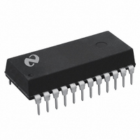
DAC1208LCJ National Semiconductor, DAC1208LCJ Datasheet - Page 9

DAC1208LCJ
Manufacturer Part Number
DAC1208LCJ
Description
IC DAC 12BIT DBL BUFF 24-DIP
Manufacturer
National Semiconductor
Series
MICRO-DAC™r
Datasheet
1.DAC1210LCJ.pdf
(18 pages)
Specifications of DAC1208LCJ
Settling Time
1µs
Number Of Bits
12
Data Interface
Parallel
Number Of Converters
1
Voltage Supply Source
Single Supply
Power Dissipation (max)
500mW
Operating Temperature
0°C ~ 70°C
Mounting Type
Through Hole
Package / Case
*
Case
DIP-24L
Lead Free Status / RoHS Status
Contains lead / RoHS non-compliant
Other names
*DAC1208LCJ
Available stocks
Company
Part Number
Manufacturer
Quantity
Price
Part Number:
DAC1208LCJ
Manufacturer:
NS/国半
Quantity:
20 000
Company:
Part Number:
DAC1208LCJ-1
Manufacturer:
ON
Quantity:
99
Application Hints
cations where the DAC is used in a continuous feedback
control loop and is driven by a binary up down counter or in
function generation circuits where a ROM is continuously
providing DAC data
Only the DAC1208 DAC1209 DAC1210 devices can have
all 12 inputs flow-through Simply grounding CS WR1 WR2
and XFER and tying Byte 1 Byte 2 high allows both internal
registers to follow the applied digital inputs (flow-through)
and directly affect the DAC analog output
1 7 Address Decoding Tips
It is possible to map the MICRO-DACs into system ROM
space to allow more efficient use of existing address decod-
ing hardware The DAC in effect can share the same ad-
dresses of any number of ROM locations The ROM outputs
will only be enabled by a READ of its address (gated by the
system READ strobe) and the DAC will only accept data
that is written to the same address (gated by the system
WRITE strobe)
The Byte 1 Byte 2 control function can easily be generated
by the processor’s least significant address bit (A0) by plac-
ing the DAC at two consecutive address locations and utiliz-
ing double-byte WRITE instructions which automatically in-
crement or decrement the address The CS and XFER sig-
nals can then be decoded from the remaining address bits
Care must be taken in selecting the actual address used
for Byte 1 of the DAC to prevent a carry (as a result of
(Continued)
First
(Byte 1)
Second
(Byte 2)
Write
Cycle
FIGURE 6 Accommodating a High Speed System
Starting with a 0 prevents a carry on address incrementing
Used as Byte 1 Byte2 Control
15
Address DAC
Decoded to
FIGURE 5
9
incrementing the address for Byte 2) from propagating
through the address word and changing any of the bits de-
coded for CS or XFER Figure 5 shows how to prevent this
effect
The same problem can occur from a borrow when an auto-
decremented address is used but only if the processor’s
address outputs are inverted before being decoded
1 8 Control Signal Timing
When interfacing these MICRO-DACs to any microproces-
sor there are two important time relationships that must be
considered to insure proper operation The first is the mini-
mum WR strobe pulse width which is specified as 320 ns for
V
typically a pulse width of only 250 ns is adequate A second
consideration is that the guaranteed minimum data hold
time of 90 ns should be met or erroneous data can be
latched This hold time is defined as the length of time data
must be held valid on the digital inputs after a qualified (via
CS) WR strobe makes a low to high transition to latch the
applied data
If the controlling device or system does not inherently meet
these timing specs the DAC can be treated as a slow mem-
ory or peripheral and utilize a technique to extend the write
strobe A simple extension of the write time by adding a
wait state can simultaneously hold the write strobe active
and data valid on the bus to satisfy the minimum WR pulse
Address Bits
CC
2
e
11 4V to 15 75V and operation over temperature but
1
0
1
0
1
0
TL H 5690-12


