DAC1218LCJ National Semiconductor, DAC1218LCJ Datasheet
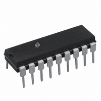
IC DAC 12BIT 18-DIP

DAC1218LCJ

Manufacturer Part Number
DAC1218LCJ
Description
IC DAC 12BIT 18-DIP
Manufacturer
National Semiconductor
Datasheet

Specifications of DAC1218LCJ

Settling Time
1µs
Number Of Bits
12
Number Of Converters
1
Voltage Supply Source
Single Supply
Power Dissipation (max)
500mW
Operating Temperature
-40°C ~ 85°C
Mounting Type
Through Hole
Package / Case
*
Case
DIP-18L
Lead Free Status / RoHS Status
Contains lead / RoHS non-compliant
Data Interface
-
Other names
*DAC1218LCJ

Available stocks

Company
Part Number
Manufacturer
Quantity
Price
Part Number:
DAC1218LCJ
Manufacturer:
ON
Quantity:
42
Part Number:
DAC1218LCJ
Manufacturer:
SIPEX
Quantity:
281
Part Number:
DAC1218LCJ
Manufacturer:
NS/国半
Quantity:
20 000
Part Number:
DAC1218LCJ-1
Manufacturer:
ON
Quantity:
19
Part Number:
DAC1218LCJ-1
Manufacturer:
MOT
Quantity:
2
C 1995 National Semiconductor Corporation
DAC1218 DAC1219
12-Bit Binary Multiplying D A Converter
General Description
The DAC1218 and the DAC1219 are 12-bit binary 4-quad-
rant multiplying D to A converters The linearity differential
non-linearity and monotonicity specifications for these con-
verters are all guaranteed over temperature In addition
these parameters are specified with standard zero and full-
scale adjustment procedures as opposed to the impractical
best fit straight line guarantee
This level of precision is achieved though the use of an
advanced silicon-chromium (SiCr) R-2R resistor ladder net-
work This type of thin-film resistor eliminates the parasitic
diode problems associated with diffused resistors and al-
lows the applied reference voltage to range from
25V independent of the logic supply voltage
CMOS current switches and drive circuitry are used to
achieve low power consumption (20 mW typical) and mini-
mize output leakage current errors (10 nA maximum)
Unique digital input circuitry maintains TTL compatible input
threshold voltages over the full operating supply voltage
range
The DAC1218 and DAC1219 are direct replacements for
the AD7541 series AD7521 series and AD7531 series with
a significant improvement in the linearity specification In
applications where direct interface of the D to A converter to
Typical Application
Ordering Information
BI-FET
TM
is a trademark of National Semiconductor Corp
Temperature Range
Linearity
Non
V
where AN
OUT
e b
AN
V
e
e
TL H 5691
REF
0 012%
0 024%
0 if digital input is low
1 if digital input is high
A1
2
a
A2
4
a
DAC1218LCJ-1
A3
0 C to
8
a
b
a
25V to
4096
A12
70 C
a microprocessor bus is desirable the DAC1208 and
DAC1230 series eliminate the need for additional interface
logic
Features
Y
Y
Y
Y
Key Specifications
Y
Y
Y
Y
Y
Y
b
Linearity specified with zero and full-scale adjust only
Logic inputs which meet TTL voltage level specs (1 4V
logic threshold)
Works with
multiplication
All parts guaranteed 12-bit monotonic
Current Settling Time
Resolution
Linearity (Guaranteed
over temperature)
Gain Tempco
Low Power Dissipation
Single Power Supply
DAC1218LCJ
DAC1219LCJ
40 C to
TL H 5691 – 1
a
85 C
g
10V reference full 4-quadrant
Connection Diagram
Package Outline
J18A Cerdip
J18A Cerdip
Dual-In-Line Package
Top View
RRD-B30M115 Printed in U S A
12 Bits (DAC1218)
11 Bits (DAC1219)
5 V
December 1994
DC
1 5 ppm C
TL H 5691– 15
to 15 V
20 mW
12 Bits
1 s
DC

Related parts for DAC1218LCJ

DAC1218LCJ Summary of contents

Page 1

... Gain Tempco Y Low Power Dissipation Y Single Power Supply Y Connection Diagram TL H 5691 – A12 4096 DAC1218LCJ-1 DAC1218LCJ DAC1219LCJ December 1994 Bits 12 Bits (DAC1218) 11 Bits (DAC1219 ppm Dual-In-Line Package TL H 5691– 15 Top View Package Outline J18A Cerdip J18A Cerdip RRD-B30M115 Printed ...

Page 2

... Digital Input Threshold Low Threshold High Threshold Digital Input Currents Digital Inputs Digital Inputs t Current Settling Time R 100 01% All Digital Inputs Switched Simultaneously Operating Conditions (Notes 1 and 2) Temperature Range DAC1218LCJ DAC1219LCJ DAC1218LCJ Range GND Voltage at Any Digital Input CC 25V 150 C a 500 mW 100 ...

Page 3

Electrical Characteristics Notes Note 1 Absolute Maximum Ratings indicate limits beyond which damage to the device may occur DC and AC electrical specifications do not apply when operating the device beyond its specified operating conditions Note 2 All voltages are ...

Page 4

Definition of Package Pinouts (A1 –A12) Digital Inputs A12 is the least significant digital input (LSB) and A1 is the most significant digital input (MSB) I DAC Current Output maximum for a OUT1 OUT1 digital input ...

Page 5

Application Hints The DAC1218 and DAC1219 are pin-for-pin compatible with the DAC1220 series but feature 12 and 11-bit linearity spec- ifications To preserve this degree of accuracy care must be taken in the selection and adjustments of the output am- ...

Page 6

Application Hints (Continued A12 OUT REF 4096 where digital input is high digital input is low e FIGURE 3 Zeroing ...

Page 7

Application Hints (Continued) FIGURE 4 Composite Output Amplifier Connection Diodes are 1N4148 FIGURE 5 DAC Settling Time Test Circuit Amplifier LM11 LF351 LF351 Composite LM11-LF351 LF356 FIGURE 6 Some Measured Settling Times C Settling Time ...

Page 8

Application Hints (Continued OBTAINING A BIPOLAR OUTPUT VOLTAGE FROM A FIXED REFERENCE The addition of a second op amp to the circuit of Figure 2 can generate a bipolar output voltage from a fixed reference voltage ( Figure ...

Page 9

Application Hints (Continued Zero and Full-Scale Adjustments The three adjustments needed for this circuit are shown in Figure 7 The first step is to set all of the digital inputs LOW (to force and then ...

Page 10

Additional Application Ideas Offsetting the Zero Code Output Voltage 2V R2 REF V e Zero Shift Amp ( 4096 (Continued) High Current Controller 5691 – 5691 – ...

Page 11

Additional Application Ideas C1 controls maximum frequency 0 5% sine wave THD over range k Range 30 kHz maximum Linearity DAC limit 4096 ( Digitally Programmable Pulse-Width Generator C(7 5V) (4096 ...

Page 12

... Physical Dimensions inches (millimeters) Order Number DAC1218LCJ-1 DAC1218LCJ or DAC1219LCJ LIFE SUPPORT POLICY NATIONAL’S PRODUCTS ARE NOT AUTHORIZED FOR USE AS CRITICAL COMPONENTS IN LIFE SUPPORT DEVICES OR SYSTEMS WITHOUT THE EXPRESS WRITTEN APPROVAL OF THE PRESIDENT OF NATIONAL SEMICONDUCTOR CORPORATION As used herein 1 Life support devices or systems are devices or ...

Related keywords