DAC1218LCJ National Semiconductor, DAC1218LCJ Datasheet - Page 6
DAC1218LCJ
Manufacturer Part Number
DAC1218LCJ
Description
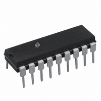
IC DAC 12BIT 18-DIP
Manufacturer
National Semiconductor
Datasheet
1.DAC1218LCJ.pdf
(12 pages)
Specifications of DAC1218LCJ
Settling Time
1µs
Number Of Bits
12
Number Of Converters
1
Voltage Supply Source
Single Supply
Power Dissipation (max)
500mW
Operating Temperature
-40°C ~ 85°C
Mounting Type
Through Hole
Package / Case
*
Case
DIP-18L
Lead Free Status / RoHS Status
Contains lead / RoHS non-compliant
Data Interface
-
Other names
*DAC1218LCJ
Available stocks
Company
Part Number
Manufacturer
Quantity
Price

Company:
Part Number:
DAC1218LCJ
Manufacturer:
SIPEX
Quantity:
281
Part Number:
DAC1218LCJ
Manufacturer:
NS/国半
Quantity:
20 000
Company:
Part Number:
DAC1218LCJ-1
Manufacturer:
ON
Quantity:
19
Company:
Part Number:
DAC1218LCJ-1
Manufacturer:
MOT
Quantity:
2


Application Hints
V
where AN
The selected amplifier should have as low an input bias
current as possible since input bias current contributes to
the current flowing through the feedback resistor BI-FET
op amps such as the LF356 or LF351 or bipolar op amps
with super
duce negligible errors
2 2 Zero and Full-Scale Adjustments
The fundamental purpose is to make the output voltages as
near 0 V
of Figure 2 by shorting out the amplifier feedback resist-
ance and adjusting the V
amp until the output reads zero volts This is done of
course with an applied digital input of all zeros if I
driving the op amp (all ones for I
is then removed and the converter is zero adjusted
A unique characteristic of these DACs is that any full-scale
or gain error is always negative This means that for a full-
scale input code the output voltage if not inherently correct
will always be less than what it should be This ensures that
adding an appropriate resistance in series with the internal
feedback resistor R
The 50
adjust the worst case DAC gain error
Conversion accuracy is only as good as the applied refer-
ence voltage so providing a source that is stable over time
and temperature is important
OUT
e b
AN
e
e
V
DC
REF
potentiometer in Figure 2 is all that is needed to
0 if digital input is low
1 if digital input is high
as possible This is accomplished in the circuit
input transistors like the LM11 or LM308A pro-
A1
2
a
A2
Fb
4
a
FIGURE 3 Zeroing an Amplifier Which Does Not Have Balancing Provisions
will always correct for any gain error
A3
8
OS
a
nulling potentiometer of the op
(Continued)
4096
A12
OUT2
) The feedback short
FIGURE 2 Unipolar Output Voltage
OUT1
TM
is
6
Figure 5 is a settling time test circuit for the complete volt-
2 3 Output Settling Time
The output voltage settling time for this circuit in response
to a change of the digital input code (a full-scale change is
the worst case) is a combination of the DAC’s output current
settling characteristics and the settling characteristics of the
output amplifier The amplifier settling is further degraded by
a feedback pole formed by the feedback resistance and the
DAC output capacitance (which varies with the digital code)
First order compensation for this pole is achieved by adding
a feedback zero with capacitor C
In many applications output response time and settling is
just as important as accuracy It can be difficult to find a
single op amp that combines excellent DC characteristics
(low V
settling time BI-FET op amps offer a reasonable compro-
mise of high speed and good DC characteristics The circuit
of Figure 4 illustrates a composite amplifier connection that
combines the speed of a BI-FET LF351 with the excellent
DC input characteristics of the LM11 If output settling time
is not so critical the LM11 can be used alone
age output DAC circuit The circuit allows the settling time of
the DAC amplifier to be measured to a resolution of 1 mV
out of a zero to
loscope Figure 6 summarizes the measured settling times
for several output amplifiers and feedback compensation
capacitors
OS
V
OS
drift and bias current) with fast response and
g
10V full-scale output change on an oscil-
TL H 5691 – 6
C
shown in Figure 2
TL H 5691 – 5
Related parts for DAC1218LCJ
Image
Part Number
Description
Manufacturer
Datasheet
Request
R

Part Number:
Description:
12-bit Binary Multiplying D/a Converter
Manufacturer:
National Semiconductor Corporation
Datasheet:

Part Number:
Description:
National Semiconductor [8-Bit D/A Converter]
Manufacturer:
National Semiconductor
Datasheet:
Part Number:
Description:
National Semiconductor [Media Coprocessor]
Manufacturer:
National Semiconductor
Datasheet:
Part Number:
Description:
Digitally Controlled Tone and Volume Circuit with Stereo Audio Power Amplifier, Microphone Preamp Stage and National 3D Sound
Manufacturer:
National Semiconductor
Datasheet:
Part Number:
Description:
Digitally Controlled Tone and Volume Circuit with Stereo Audio Power Amplifier, Microphone Preamp Stage and National 3D Sound
Manufacturer:
National Semiconductor
Datasheet:
Part Number:
Description:
AC97 Rev 2 Codec with Sample Rate Conversion and National 3D Sound
Manufacturer:
National Semiconductor
Part Number:
Description:
Manufacturer:
National Semiconductor
Datasheet:
Part Number:
Description:
Manufacturer:
National Semiconductor
Datasheet:
Part Number:
Description:
General Purpose, Low Voltage, Low Power, Rail-to-Rail Output Operational Amplifiers
Manufacturer:
National Semiconductor
Datasheet:
Part Number:
Description:
8-bit 20 MSPS flash A/D converter.
Manufacturer:
National Semiconductor
Datasheet:
Part Number:
Description:
Low Noise Quad Operational Amplifier
Manufacturer:
National Semiconductor
Datasheet:
Part Number:
Description:
Quad Differential Line Receivers
Manufacturer:
National Semiconductor
Datasheet:
Part Number:
Description:
Quad High Speed Trapezoidal? Bus Transceiver
Manufacturer:
National Semiconductor
Datasheet:
Part Number:
Description:
Dual Line Receiver
Manufacturer:
National Semiconductor
Datasheet: