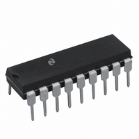
DAC1218LCJ National Semiconductor, DAC1218LCJ Datasheet - Page 9

DAC1218LCJ
Manufacturer Part Number
DAC1218LCJ
Description
IC DAC 12BIT 18-DIP
Manufacturer
National Semiconductor
Datasheet
1.DAC1218LCJ.pdf
(12 pages)
Specifications of DAC1218LCJ
Settling Time
1µs
Number Of Bits
12
Number Of Converters
1
Voltage Supply Source
Single Supply
Power Dissipation (max)
500mW
Operating Temperature
-40°C ~ 85°C
Mounting Type
Through Hole
Package / Case
*
Case
DIP-18L
Lead Free Status / RoHS Status
Contains lead / RoHS non-compliant
Data Interface
-
Other names
*DAC1218LCJ
Available stocks
Company
Part Number
Manufacturer
Quantity
Price
Company:
Part Number:
DAC1218LCJ
Manufacturer:
SIPEX
Quantity:
281
Part Number:
DAC1218LCJ
Manufacturer:
NS/国半
Quantity:
20 000
Company:
Part Number:
DAC1218LCJ-1
Manufacturer:
ON
Quantity:
19
Company:
Part Number:
DAC1218LCJ-1
Manufacturer:
MOT
Quantity:
2
Figure 7 The first step is to set all of the digital inputs LOW
Application Hints
3 1 Zero and Full-Scale Adjustments
The three adjustments needed for this circuit are shown in
(to force I
volts at the inverting input (pin 2) of OA1 Next with a code
of all zeros still applied adjust ‘‘- full-scale adjust’’ the refer-
ence voltage for V
output voltage will be opposite that of the applied reference
Finally set all of the digital inputs HIGH and adjust ‘‘
scale adjust’’ for V
output at this time will be the same as that of the reference
voltage This
count the effects of the V
offset is less than 0 1% of V
external resistor mismatch
Additional Application Ideas
For the circuits shown D represents the decimal equivalent of the binary digital input code D ranges from 0 (for an all zeros
input code) to 4095 (for an all ones input code) and for any code can be determined from
D
e
2048(A1)
OUT1
a
to 0) and then trim ‘‘zero adjust’’ for zero
full-scale adjustment scheme takes into ac-
where AN
a
OUT
OUT
1024(A2)
AN
e
e
OS
V
REF
e
g
e
REF
of amplifier A2 (as long as this
l
(Continued)
(ideal V
0 if that input is low
1 if that input is high
a
(511 512) The sign of the
) and any gain errors due to
512(A2)
REF
DAC Controlled Amplifier
)
l
a
The sign of the
2(A11)
a
full-
a
1(A12)
9
4 0 MISCELLANEOUS APPLICATION HINTS
The devices are CMOS products and reasonable care
should be exercised in handling them to prevent catastroph-
ic failures due to electrostatic discharge
During power-up supply voltage sequencing the negative
supply of the output amplifier may appear first This will typi-
cally cause the output of the op amp to bias near the nega-
tive supply potential No harm is done to the DAC however
as the on-chip 15 k
current flow from I
diode drop below ground
As a general rule any unused digital inputs should be tied
high or low as required by the application As a trouble-
shooting aid if any digital input is left floating the DAC will
interpret that input as a logical 1 level
OUT1
feedback resistor sufficiently limits the
when this lead is clamped to one
TL H 5691 – 10


