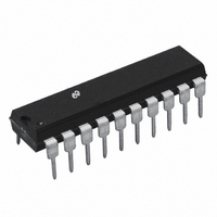
DAC1232LCJ National Semiconductor, DAC1232LCJ Datasheet - Page 2

DAC1232LCJ
Manufacturer Part Number
DAC1232LCJ
Description
IC DAC 12BIT DBL BUFFERED 20-DIP
Manufacturer
National Semiconductor
Series
MICRO-DAC™r
Datasheet
1.DAC1210LCJ.pdf
(18 pages)
Specifications of DAC1232LCJ
Settling Time
1µs
Number Of Bits
12
Data Interface
Parallel
Number Of Converters
1
Voltage Supply Source
Single Supply
Power Dissipation (max)
500mW
Operating Temperature
-40°C ~ 85°C
Mounting Type
Through Hole
Package / Case
*
Case
DIP-20L
Lead Free Status / RoHS Status
Contains lead / RoHS non-compliant
Other names
*DAC1232LCJ
Available stocks
Company
Part Number
Manufacturer
Quantity
Price
Company:
Part Number:
DAC1232LCJ
Manufacturer:
NS
Quantity:
5 510
Part Number:
DAC1232LCJ
Manufacturer:
NS/国半
Quantity:
20 000
Company:
Part Number:
DAC1232LCJ-1
Manufacturer:
ON
Quantity:
121
Resolution
Linearity Error
(End Point Linearity)
Differential Non-Linearity
Monotonicity
Gain Error (Min)
Gain Error (Max)
Gain Error Tempco
Power Supply Rejection
Reference Input Resistance (Min)
Reference Input Resistance (Max)
Output Feedthrough Error
Output Capacitance
Supply Current Drain
Output Leakage Current
Digital Input Threshold
Digital Input Currents
Absolute Maximum Ratings
If Military Aerospace specified devices are required
please contact the National Semiconductor Sales
Office Distributors for availability and specifications
(Notes 1 and 2)
Supply Voltage (V
Voltage at Any Digital Input
Voltage at V
Storage Temperature Range
Package Dissipation at T
DC Voltage Applied to I
ESD Susceptability
Electrical Characteristics
V
Note 13) all other limits T
I
I
OUT1
OUT2
REF
(Note 3)
(Note 4)
e
10 000 V
Parameter
REF
Input
DC
CC
)
V
CC
OUT1
A
e
e
A
11 4 V
25 C
e
or I
T
OUT2
J
DC
e
Zero and Full-Scale
Adjusted
DAC1208 DAC1230
DAC1209 DAC1231
DAC1210 DAC1232
Zero and Full-Scale
Adjusted
DAC1208 DAC1230
DAC1209 DAC1231
DAC1210 DAC1232
Using Internal R
V
All Digital Inputs
Latched High
V
All Data Inputs Latched
Low
All Data Inputs I
Latched High
All Data Inputs I
Latched Low
All Data Inputs Latched
Low
All Data Inputs Latched
High
Low Threshold
High Threshold
Digital Inputs
Digital Inputs
to 15 75 V
ref
REF
25 C
e
b
e
b
65 C to
g
20 Vp-p f
Conditions
100 mV to V
10V
V
DC
CC
k
l
g
a
500 mW
0 8V
2 2V
unless otherwise noted Boldface limits apply from T
to GND
Fb
17 V
1V
I
I
g
150 C
e
OUT1
OUT2
OUT1
OUT2
800V
25V
100 kHz
DC
CC
2
4 7 13
4 7 13
Operating Conditions
Lead Temperature (Soldering 10 sec )
Temperature Range
Range of V
Voltage at Any Digital Input
Notes
11 13
11 13
13
13
13
13
13
13
DAC1208LCJ DAC1209LCJ
DAC1210LCJ DAC1230LCJ
DAC1231LCJ DAC1232LCJ
DAC1231LIN DAC1232LIN
DAC1208LCJ-1 DAC1210LCJ-1
DAC1230LCJ-1 DAC1231LCJ-1
DAC1232LCJ-1 DAC1231LCN
DAC1232LCN DAC1231LCWM
DAC1232LCWM
4
7
7
7
7
9
(Note 10)
CC
b
b
g
g
Typ
3 0
0 1
0 1
12
12
15
15
0 1
0 1
1 3
3 0
g
g
g
g
g
g
(Note 5)
Tested
b
Limit
0 018
0 024
0 050
0 018
0 024
0 050
b
g
0 8
2 2
12
12
10
20
15
15
10
0 0
2 0
200
0 2
30
g
g
g
g
(Note 6)
Design
g
g
b
g
b
Limit
0 018
0 024
0 018
0 024
200
200
2 5
0 8
2 2
0 05
0 05
12
12
10
20
15
15
10
200
70
70
6 0
40 C
0 C
T
4 75 V
MIN
MIN s
s
s
to T
T
T
DC
ppm of FSR V
ppm of FS C
V
A s
A s
T
CC
% of FSR
% of FSR
% of FSR
% of FSR
% of FSR
% of FSR
% of FSR
% of FSR
A s
to 16 V
MAX
mVp-p
Units
V
V
to GND
Bits
Bits
mA
a
a
k
nA
nA
pF
pF
pF
pF
A
A
300 C
DC
DC
T
DC
DC
85 C
70 C
(see
MAX
DC


